Silicon-penetrating through hole with control electrode and manufacturing method thereof
A technology of through-silicon vias and control circuits, which is applied to circuits, electrical components, and electrical solid-state devices, and can solve problems such as increasing the complexity of chip manufacturing processes
- Summary
- Abstract
- Description
- Claims
- Application Information
AI Technical Summary
Problems solved by technology
Method used
Image

Examples
Embodiment Construction
[0029] In order to enable those skilled in the art of the present invention to further understand the present invention, the following description lists several preferred embodiments of the present invention, together with the accompanying drawings and descriptions, to describe in detail the content of the present invention and the desired effect .
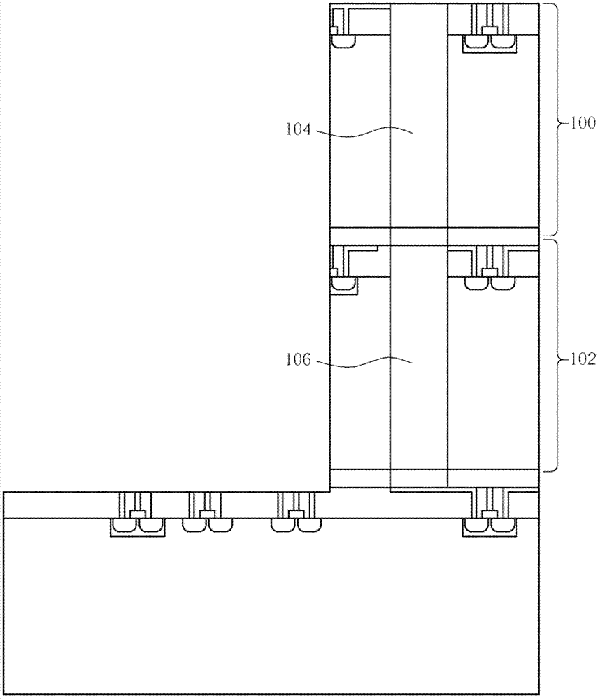
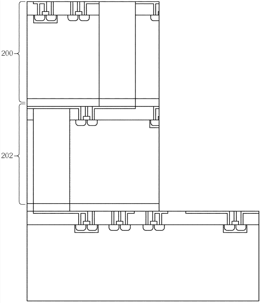
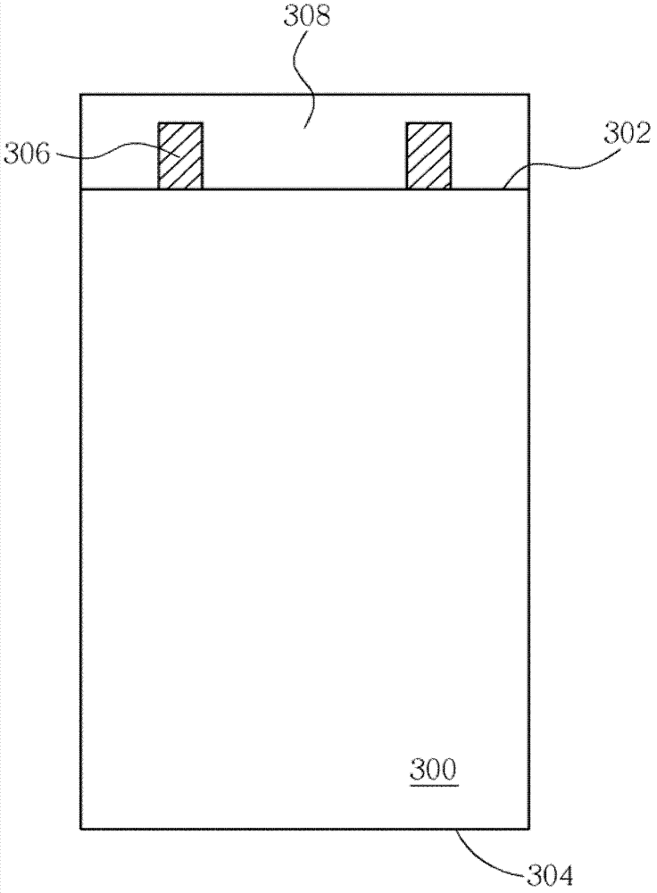
[0030] Please refer to Figure 3 to Figure 9 , which is a schematic diagram showing the steps of the manufacturing method of the TSV with the control circuit in the present invention. Such as image 3 As shown, a substrate 300 is firstly provided, such as a silicon substrate, an epitaxial silicon substrate, a silicon germanium substrate, a silicon carbide substrate or a silicon-covered insulating ( silicon-on-insulator, SOI). The substrate 300 has a first surface 302 and a second surface 304 . The first surface 302 is, for example, the active surface of the substrate 300 , and the second surface 304 is, for example, the back s...
PUM
 Abstract
Description
Claims
Application Information
 - R&D
- Intellectual Property
- Life Sciences
- Materials
- Tech Scout
- Unparalleled Data Quality
- Higher Quality Content
- 60% Fewer Hallucinations
Browse by: Latest US Patents, China's latest patents, Technical Efficacy Thesaurus, Application Domain, Technology Topic, Popular Technical Reports.
© 2025 PatSnap. All rights reserved.Legal|Privacy policy|Modern Slavery Act Transparency Statement|Sitemap|About US| Contact US: help@patsnap.com