Active device and active device array substrate

A technology of active components and array substrates, applied in electrical components, electric solid-state devices, semiconductor devices, etc., which can solve the problem of reduced component area, high brightness of pixel aperture ratio, easy current attenuation of double gate structure, limited effect of on-current boost, etc. problem, to achieve the effect of increasing the pixel aperture ratio, solving the incompatibility between driving capability and aperture ratio, and reducing the circuit layout space

Inactive Publication Date: 2013-10-23
DONGGUAN MASSTOP LIQUID CRYSTAL DISPLAY +1
View PDF3 Cites 34 Cited by
  • Summary
  • Abstract
  • Description
  • Claims
  • Application Information

AI Technical Summary

Problems solved by technology

However, the double gate structure needs to include thin film transistors with front channel and back channel. The back channel is easy to cause damage to the channel layer during the manufacturing process, so the current of the double gate structu...

Method used


Image

  • Active device and active device array substrate
  • Active device and active device array substrate
  • Active device and active device array substrate

Examples


Embodiment Construction

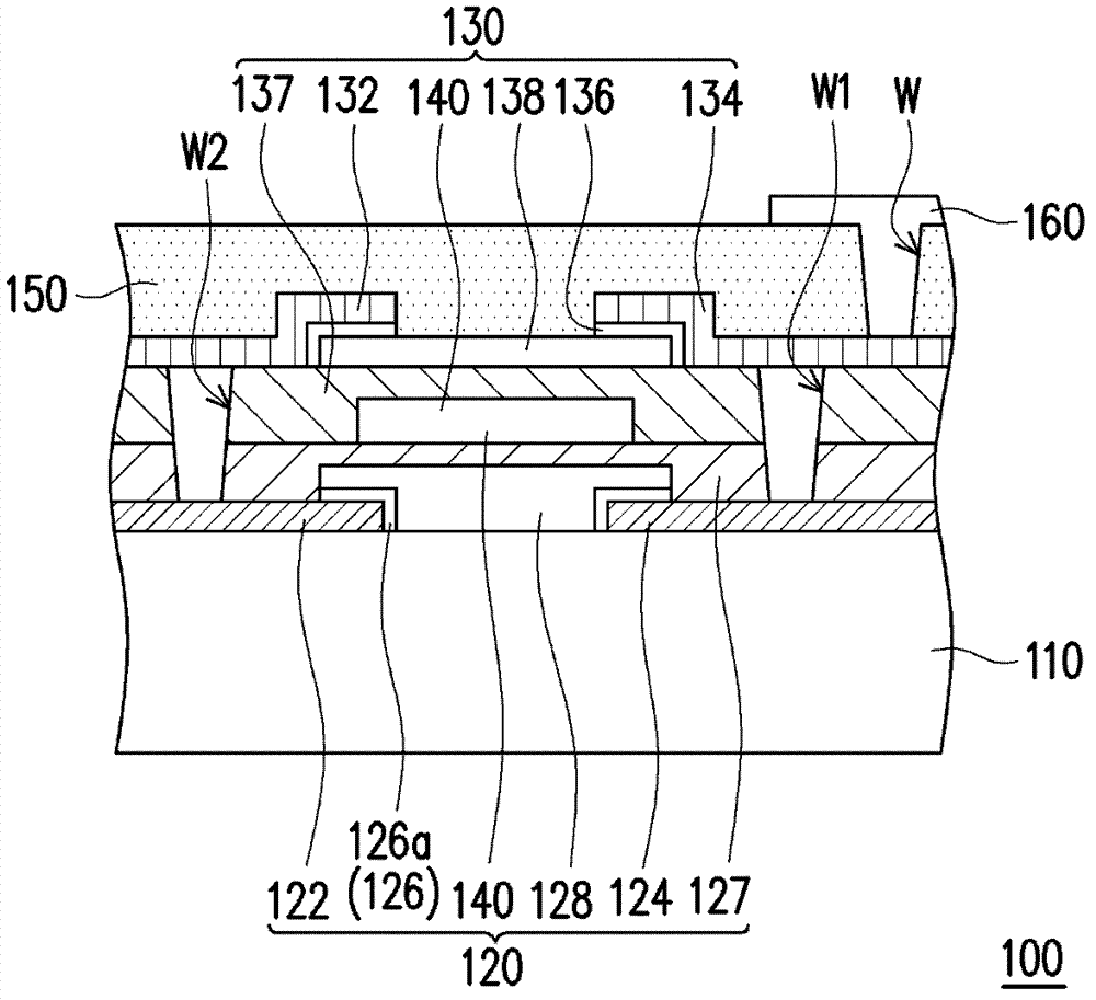
[0049] figure 1 It is a schematic cross-sectional view of the active device array substrate according to the first embodiment of the present invention. Please refer to figure 1 The active device array substrate 100 of this embodiment includes a substrate 110 , a first transistor 120 , a second transistor 130 , a common gate 140 , a protective layer 150 and a pixel electrode 160 . The first transistor 120 is located on the substrate 110 , wherein the first transistor 120 has a first channel layer 128 . The second transistor 130 is stacked on the first transistor 120 , wherein the second transistor 130 has a second channel layer 138 . The first transistor 120 and the second transistor 130 share the same common gate 140 , and the common gate 140 is located between the first channel layer 128 and the second channel layer 138 .

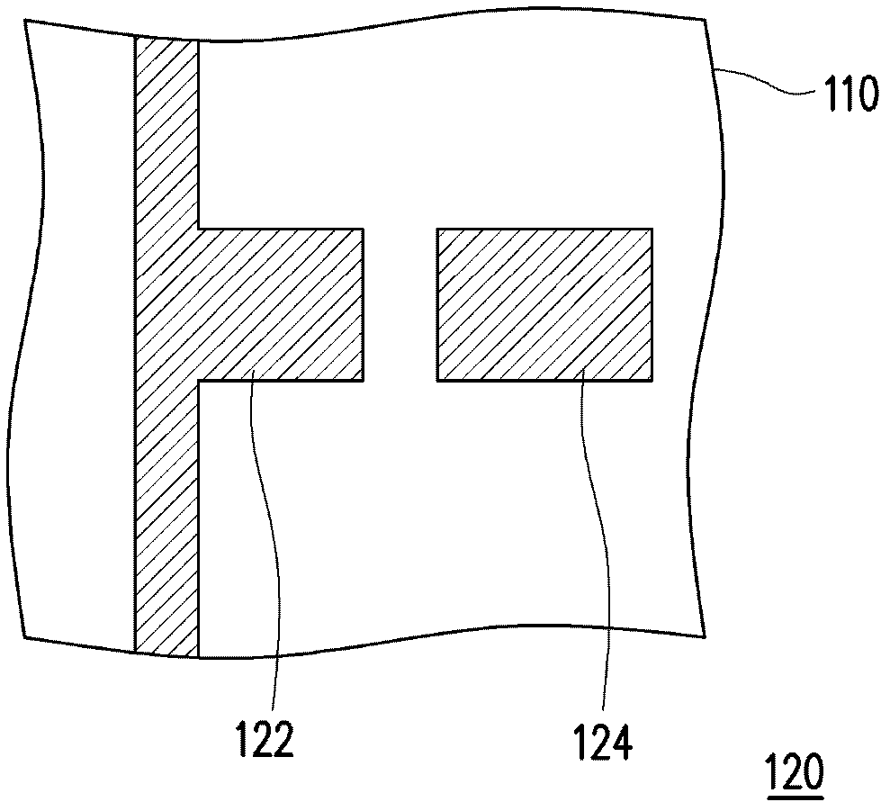
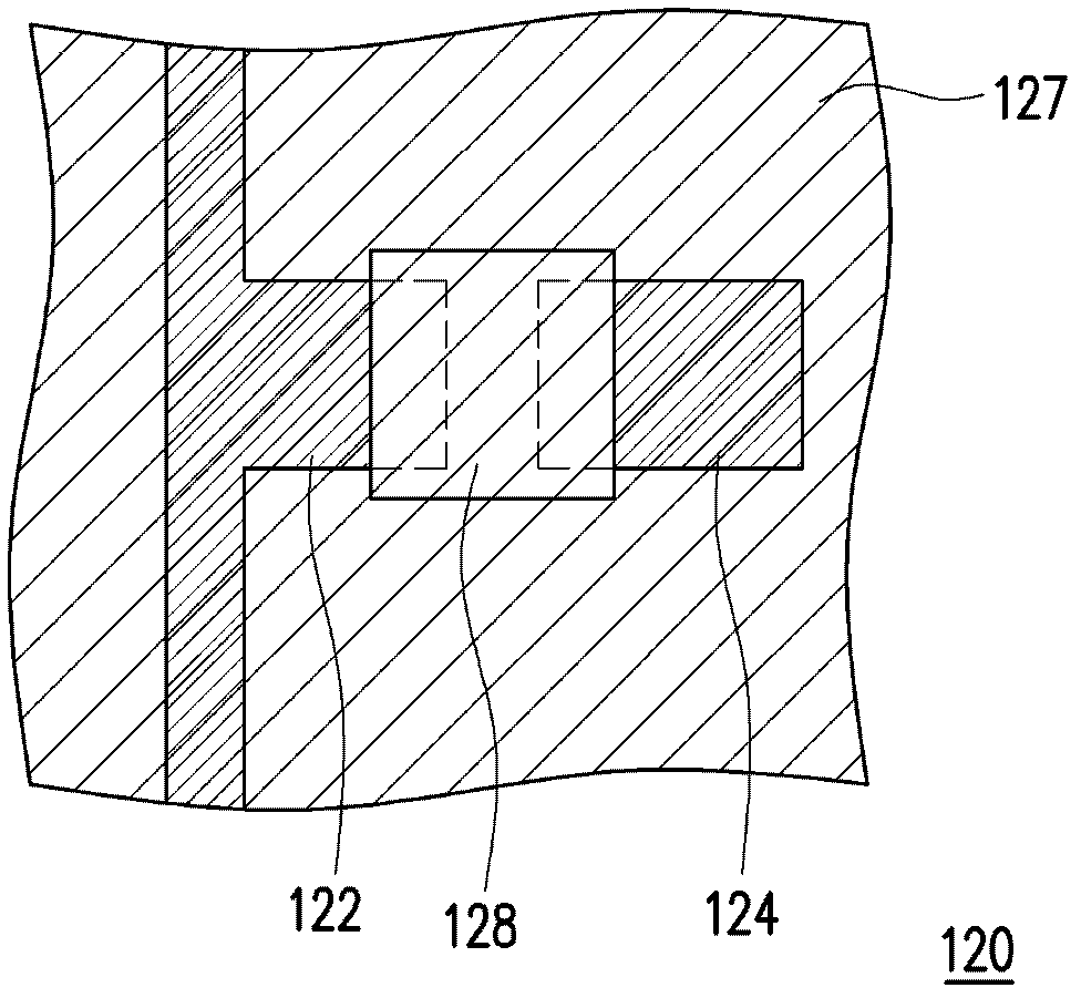
[0050] Specifically, the first transistor 120 includes a first source 122 , a first drain 124 , a first doped amorphous silicon layer 126 and a first g...


PUM


Abstract

The invention provides an active device and an active device array substrate. The active device array substrate comprises a substrate and a plurality of active devices located on the substrate. At least one of the active devices comprises a first transistor and a second transistor, wherein the first transistor is located on the substrate and provided with a first channel layer; the second transistor is stacked on the first transistor and provided with a second channel layer; the first transistor and the second transistor share a common grid electrode; and the common grid electrode is located between the first channel layer and the second channel layer.

Description

technical field [0001] The present invention relates to an active element and an active element array substrate, and in particular to a dual-channel active element and an active element array substrate. Background technique [0002] In recent years, with the rapid development of electronic technology, thin film transistor liquid crystal display (Thin Film Transistor Liquid Crystal Display, TFT LCD) with superior characteristics such as high image quality, good space utilization efficiency, low power consumption, and no radiation has gradually become the market choice. mainstream. [0003] With the requirement of large-area and high-resolution thin-film transistor liquid crystal displays, thin-film transistors must have high-mobility carriers, thus driving thin-film transistors to shorten their charge and discharge times. Generally, considering high mobility, high stability and low cost, the semiconductor layer of the TFT in the driving circuit can be made of amorphous silic...

Claims


Application Information

Patent Timeline
IPC IPC(8): H01L27/02H01L29/786
Inventor 叶政谚陈昱廷
Owner DONGGUAN MASSTOP LIQUID CRYSTAL DISPLAY
Why Eureka
Try Eureka