Solid-state imaging device and manufacturing method of solid-state imaging device

A technology of solid-state imaging and manufacturing methods, which is applied in the direction of electric solid-state devices, radiation control devices, semiconductor devices, etc., can solve the problem of increasing the amount of charge, and achieve the effect of increasing the amount of charge

Active Publication Date: 2013-10-23
KK TOSHIBA
View PDF1 Cites 2 Cited by
  • Summary
  • Abstract
  • Description
  • Claims
  • Application Information

AI Technical Summary

Problems solved by technology

[0005] However, in order to further reliably suppress the generation of dark current, the amount of charge in the fixed charge layer must be further increased

Method used


Image

  • Solid-state imaging device and manufacturing method of solid-state imaging device
  • Solid-state imaging device and manufacturing method of solid-state imaging device
  • Solid-state imaging device and manufacturing method of solid-state imaging device

Examples


no. 1 Embodiment approach

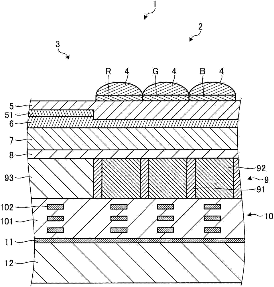
[0022] In the present embodiment, as an example of a solid-state imaging device, a so-called back-illuminated CMOS (Complementary Metal Oxide) in which a wiring layer is formed on the surface opposite to the surface on which the incident light enters the surface of the light-receiving portion that converts incident light to photoelectricity will be described. Semiconductor, Complementary Metal Oxide Semiconductor) image sensor.

[0023] In the following, the case where the back-illuminated CMOS image sensor photoelectrically converts incident light into negative charges is described, but the back-illuminated CMOS image sensor according to the embodiment may be configured to photoelectrically convert incident light into positive charges.

[0024] In addition, the solid-state imaging device of this embodiment is not limited to a back-illuminated CMOS image sensor, and may be any image sensor such as a surface-illuminated CMOS image sensor and / or a CCD (Charge Coupled Device) imag...

no. 2 Embodiment approach

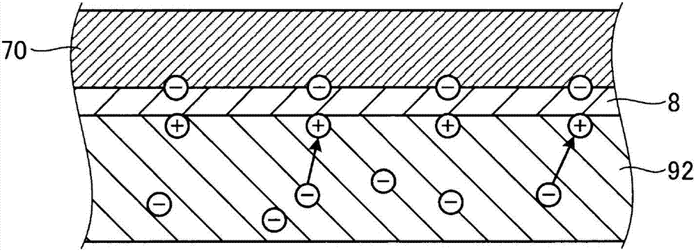
[0071] Next, the CMOS sensor of the second embodiment will be described. The difference between the CMOS sensor of this embodiment and the CMOS sensor 1 of the first embodiment is that the structure of the fixed charge layer is different. Therefore, here, refer to Figure 4 The fixed charge layer 7a of this embodiment will be described, and the description of other components in the CMOS sensor will be omitted.

[0072] Figure 4 It is an explanatory diagram of the cross section of the fixed charge layer 7a of the second embodiment. In addition, in the following description, Figure 4 Among the components shown are Figure 3B Components that are the same as those shown are assigned the same symbols, and their descriptions are omitted.

[0073] Such as Figure 4 As shown, the fixed charge layer 7a has a second charge holding film 72a that holds negative charges on the light incident surface side of the first charge holding film 71, and has a negative charge holding film 7...


PUM


Abstract

A solid-state imaging device according to embodiments of the present disclosure includes a light receiving unit, a first charge holding film, and a second charge holding film. The light receiving unit converts the incident light to an electric current. The first charge holding film is formed above the light receiving unit and holds electric charges. The second charge holding film is formed on the first charge holding film and holds electric charges. Further, concentration of oxygen in the second charge holding film is higher than concentration of oxygen in the first charge holding film.

Description

technical field [0001] Embodiments of the present invention relate to a solid-state imaging device and a method of manufacturing the solid-state imaging device. Background technique [0002] Conventionally, in solid-state imaging devices, it is detected that a current (hereinafter referred to as "dark current") is formed by charges existing in the light-receiving part regardless of the presence or absence of incident light incident on the light-receiving part for photoelectrically converting the incident light, and an image is taken. There is a problem with images that are brighter than they actually are. [0003] Therefore, when the charge generated by photoelectric conversion is negative charge, a solid-state imaging device that suppresses the generation of dark current by forming a fixed charge layer holding negative charge on the top surface side of the light-receiving part is conceivable. In this solid-state imaging device, positive charges in the light receiving porti...

Claims


Application Information

Patent Timeline
IPC IPC(8): H01L27/146
CPCH01L31/18H01L27/1464H01L27/14643H01L31/02H01L27/146H01L27/14627H01L31/0216
Inventor 上村昌己宇家真司工藤知靖
Owner KK TOSHIBA
Why Eureka
Try Eureka