LED (Light Emitting Diode) packaging structure and process

An LED packaging and process technology, applied in electrical components, electrical solid-state devices, circuits, etc., can solve the problems of low light output and low adhesion of LED chips, shorten the baking and curing time, improve production efficiency, and save production. cost effect

Active Publication Date: 2013-10-23
LEDMAN OPTOELECTRONICS
View PDF3 Cites 10 Cited by
  • Summary
  • Abstract
  • Description
  • Claims
  • Application Information

AI Technical Summary

Problems solved by technology

[0004] Based on this, it is necessary to provide an LED packaging process for the problems of low adhesion between the existing fluorescent adhesive layer and the LED chip and the low light output rate of the LED chip.

Method used


Image

  • LED (Light Emitting Diode) packaging structure and process
  • LED (Light Emitting Diode) packaging structure and process
  • LED (Light Emitting Diode) packaging structure and process

Examples


Embodiment Construction

[0035] The present invention will be further described below in conjunction with the drawings.

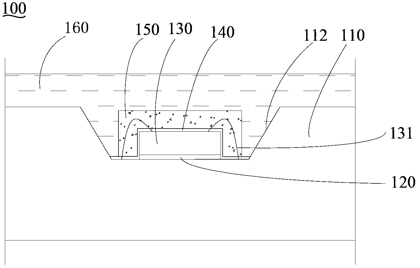
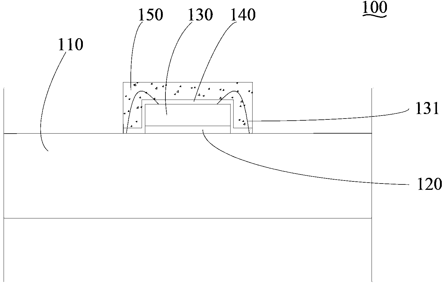
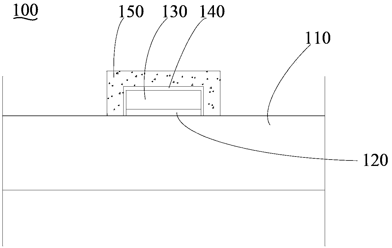
[0036] See figure 1 , An LED packaging structure 100 includes a bracket 110, a die bonding layer 120, an LED chip 130, a primer layer 140, an elastic fluorescent glue layer 150, and a packaging glue layer 160.

[0037] The bracket 110 is provided with a bowl and cup structure 112. The bottom of the bowl structure 112 is a die bonding area. The bowl-cup structure 112 can improve the light-emitting effect of the LED packaging structure 100 to a certain extent, and when the LED packaging structure 100 needs to be filled with packaging glue, the bowl-cup structure 112 is convenient for filling with packaging glue.

[0038] It can be understood that the bowl structure 112 can be omitted. See figure 2 , The surface of the support 110 is provided with a die bonding area.

[0039] The die bonding layer 120 is coated on the surface of the die bonding zone. The die bonding layer 120 is used to f...


PUM

PropertyMeasurementUnit
thicknessaaaaaaaaaa

Abstract

The invention relates to an LED (Light Emitting Diode) packaging process, which comprises the following steps of preparing an elastic fluorescent gel layer: pouring evenly-agitated mixture of organic silica gel and fluorescence powder into a mold, baking the mold which contains the mixture of the organic silica gel and the fluorescence powder and taking down the mold after molding through baking to obtain the jelly elastic fluorescent gel layer; coating a die bonding layer: coating the die bonding layer in a die bonding area of a stent and bonding an LED chip with the die bonding layer; covering with the elastic fluorescent gel layer and press-fitting the elastic fluorescent gel layer on the LED chip to enable the LED chip to be accommodated in the elastic fluorescent gel layer; and baking for solidification: baking the LED structure covered by the elastic fluorescent gel layer to enable the elastic fluorescent gel layer to be solidified to become an elastic fluorescent layer which is then closely bonded with the stent and the LED chip. The LED chip is enabled to be capable of uniformly emit light, the luminous efficiency is higher, and the brightness and the luminous effect of the LED chip are guaranteed. The invention additionally provides an LED packaging structure.

Description

Technical field [0001] The present invention relates to the technical field of LED packaging, in particular to an LED packaging structure and process. Background technique [0002] As the fourth-generation green lighting source, LED has been widely used and is an indispensable lighting tool for industry and life. [0003] Generally, the LED packaging adopts a glue dispensing method or a fluorescent glue film on the surface of the LED chip. In the traditional way of placing the fluorescent film on the surface of the LED chip, firstly, the fluorescent film is made in advance, and the fluorescent film is attached to the surface of the chip, or it is made into a hollow shape to cover the chip. Since the cured fluorescent film has a certain hardness, it affects the bonding degree between the fluorescent film and the chip, thereby affecting the light extraction rate of the LED chip. Summary of the invention [0004] Based on this, it is necessary to provide an LED packaging process for ...

Claims


Application Information

Patent Timeline
Patent Type & Authority Applications(China)
IPC IPC(8): H01L33/50H01L33/48
CPCH01L2224/48091H01L2924/181H01L2924/00014H01L2924/00012
Inventor 李漫铁屠孟龙李扬林
Owner LEDMAN OPTOELECTRONICS
Why Eureka
Try Eureka