

Image sensor and manufacturing method of image sensor
A technology of an image sensor and a manufacturing method, which is applied in the field of semiconductors, can solve the problems of low transmission efficiency of photogenerated carriers, achieve high transmission rate and improve transmission efficiency
- Summary
- Abstract
- Description
- Claims
- Application Information
AI Technical Summary
Problems solved by technology
Method used
Image

Examples
Embodiment Construction
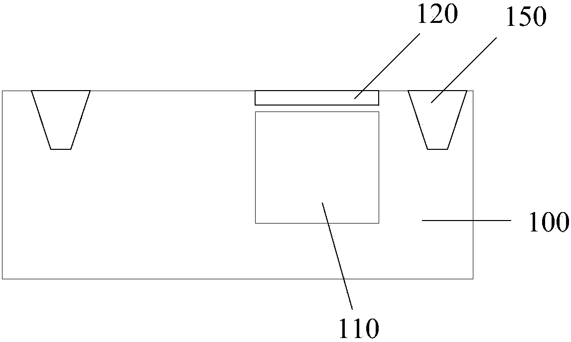
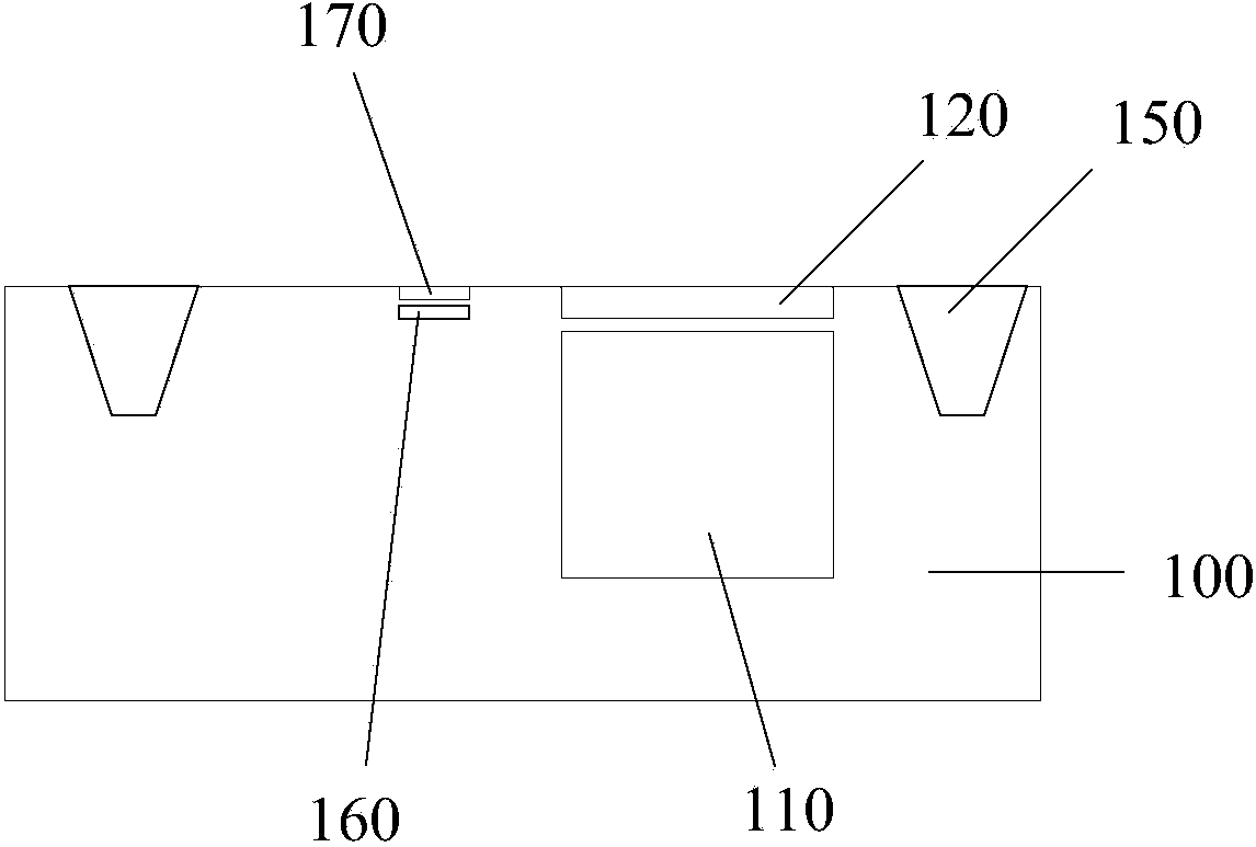
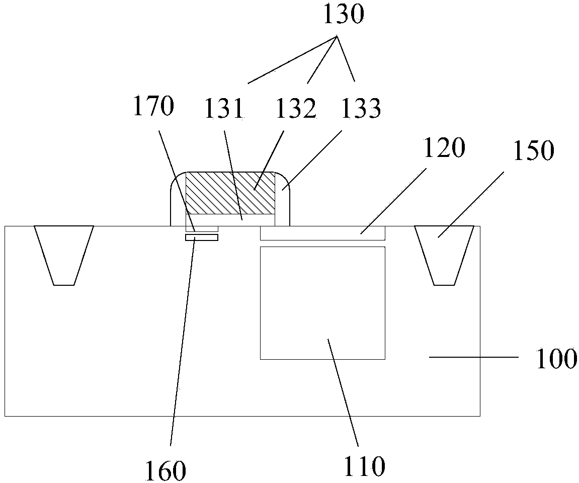
[0037] In existing image sensors, since the floating diffusion region is a heavily doped region, the transmission efficiency of photogenerated carriers is limited, and the transmission efficiency of photogenerated carriers is low.
[0038] To this end, the present invention provides an image sensor. The image sensor is provided with a lightly doped region of the second conductivity type in the semiconductor substrate of the first conductivity type under the gate, and the lightly doped region of the second conductivity type In contact with the floating diffusion region, the lightly doped region of the second conductivity type is equivalent to the epitaxial part of the floating diffusion region, so that when the photogenerated carriers are transported in the channel, they are easily absorbed by the second conductive type due to the potential in the transmission channel. Type doped region and its adjacent floating diffusion region attract, the transport rate of photogenerated carr...
PUM
 Abstract
Description
Claims
Application Information