An address mapping method in the flash memory translation layer of a solid-state disk

An address mapping and translation layer technology, applied in the direction of memory address/allocation/relocation, etc., can solve the problems of directly updating data blocks, unable to ensure the integrity and correctness of data in data blocks, and limited erasure times of storage units

Active Publication Date: 2016-01-20
NAT UNIV OF DEFENSE TECH
View PDF3 Cites 0 Cited by
  • Summary
  • Abstract
  • Description
  • Claims
  • Application Information

AI Technical Summary

Problems solved by technology

[0004]1. Erase before write mechanism, that is, when rewriting new data to a data block that has already been written, NAND Flash cannot directly update the original data block like a disk , but the data block needs to be erased and then rewritten with new data
[0005]2. The number of erasing of a single storage unit is limited, that is, the number of times of erasing each data block (Block) in NAND Flash is limited. After the number of times, the integrity and correctness of the data stored in the data block cannot be guaranteed
Therefore, according to the characteristics of NAND Flash, how to effectively use the principle of time locality and space locality of the load to improve the hit rate of page mapping information in the SRAM cache and finally improve the efficiency of the flash conversion layer has become a key technology to be solved urgently Problem, there is no effective design method to improve the efficiency of the flash translation layer by synergistically using the principle of load time locality and space locality in the existing technology

Method used


Image

  • An address mapping method in the flash memory translation layer of a solid-state disk
  • An address mapping method in the flash memory translation layer of a solid-state disk
  • An address mapping method in the flash memory translation layer of a solid-state disk

Examples


Embodiment Construction

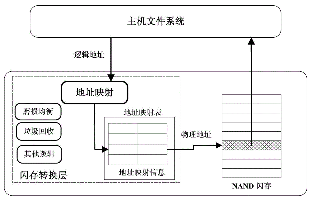
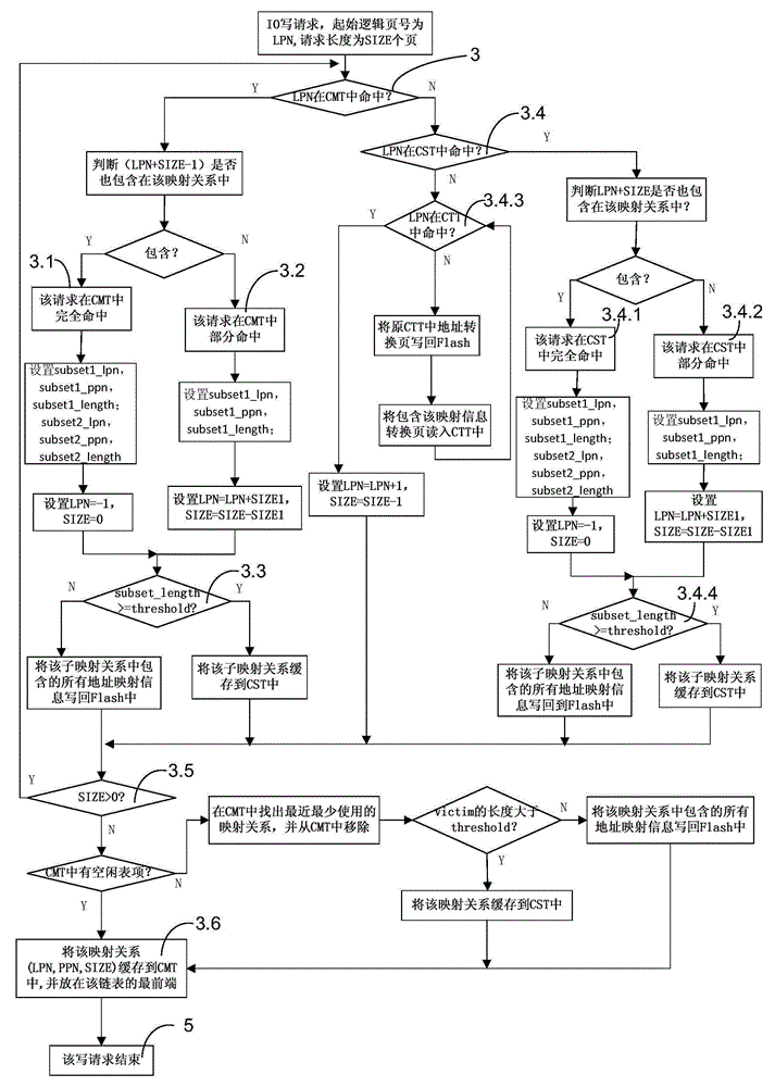
[0055] The implementation steps of the address mapping method in the flash memory translation layer of the solid state disk in this embodiment are as follows:

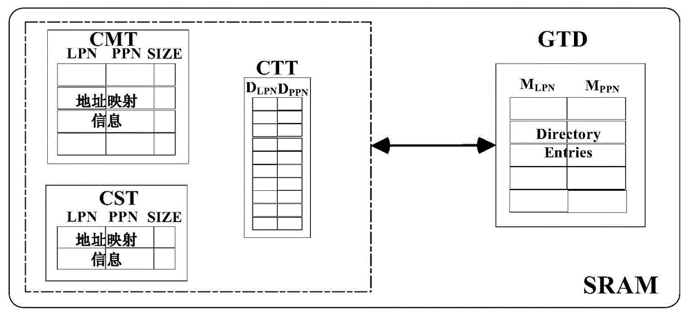
[0056] 1) Establish the cache mapping table (CachedMappingTable, CMT), cache split table (CachedSplitTable, CST), cache translation table (CachedTranslationTable, CTT) and global translation directory (GlobalTranslationDirectory, GTD) in the SRAM of the solid-state disk in advance, and the cache mapping table CMT The cache split table CST has three entry fields: the start logical page number (LogicalPageNumber, LPN), the start physical page number (PhysicalPageNumber, PPN), and the length (SIZE). The cache conversion table CTT has a logical page number D LPN and physical page number D PPN A total of two entry fields, the global translation directory GTD has a logical page number M LPN , logical page number M LPN The physical page number M stored in the SSD Flash PPN A total of two entry fields.

[0057] like figu...


PUM


Abstract

The invention discloses an address mapping method in a flash memory conversion layer of a solid-state disk. The implementation steps are as follows: 1) Establish a cache mapping table, a cache split table, a cache conversion table and a global conversion directory in SRAM in advance; 2) Receive an IO request , if it is a write request, skip to step 3), otherwise, skip to step 4); 3) first search the hit status of the current IO request in the SRAM table, complete the write operation according to the hit mapping information, and according to the hit type and valve The value size caches the mapping information; 4) Prioritizes the hit status of the current IO request in the SRAM table, and completes the read operation through the hit mapping information in the SRAM. The present invention has the advantages of being able to improve the random write performance of the solid-state disk while prolonging the service life of the solid-state disk, high efficiency of the flash conversion layer, high hit rate of address mapping information in the SRAM, and less additional read and write operations between the SRAM and the solid-state disk Flash .

Description

technical field [0001] The invention relates to the technical field of solid-state disk storage, in particular to an address mapping method in a flash memory translation layer of a solid-state disk. Background technique [0002] NAND Flash-based Solid State Drive (SSD) is a non-volatile computer storage device, which can effectively improve the performance of the storage system by virtue of its low latency, low power consumption, high reliability and other advantages. In the field of enterprise and consumer storage, solid-state disks are gradually replacing traditional mechanical hard disks, and the development of high-performance solid-state disk systems has become a research hotspot in the current storage field. [0003] NAND Flash has three basic operations of reading, writing, and erasing, and its main features are described as follows: [0004] 1. Erase before write mechanism, that is, when rewriting new data to a data block that has already been written, NAND Flash ca...

Claims


Application Information

Patent Timeline
Patent Type & Authority Patents(China)
IPC IPC(8): G06F12/06G06F12/02
CPCG06F2212/7201G06F12/0246G06F2212/1036G06F2212/1016
Inventor 肖立权宋振龙魏登萍李琼郑义谢徐超李元山黎铁军张晓明方健王辉邓峰伍玉良
Owner NAT UNIV OF DEFENSE TECH
Why Eureka
Try Eureka