Method for manufacturing semiconductor device

A device manufacturing method and semiconductor technology, which are applied in semiconductor/solid-state device manufacturing, electrical components, circuits, etc., can solve problems such as crystal structure damage, reduction effect, and influence on source-drain epitaxial growth of silicon germanium.

Active Publication Date: 2013-12-04
INST OF MICROELECTRONICS CHINESE ACAD OF SCI
View PDF5 Cites 14 Cited by
  • Summary
  • Abstract
  • Description
  • Claims
  • Application Information

AI Technical Summary

Problems solved by technology

[0004] The current problem is that if HALO implantation is performed before epitaxy, high dose implantation will cause damage to the crystal structure at the surface of the source and drain grooves, thereby affecting the subsequent source and drain epitaxial g

Method used


Image

  • Method for manufacturing semiconductor device
  • Method for manufacturing semiconductor device
  • Method for manufacturing semiconductor device

Examples


Embodiment Construction

[0020] Hereinafter, the present invention is described by means of specific embodiments shown in the drawings. It should be understood, however, that these descriptions are exemplary only and are not intended to limit the scope of the present invention. Also, in the following description, descriptions of well-known structures and techniques are omitted to avoid unnecessarily obscuring the concept of the present invention.

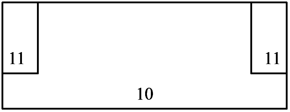
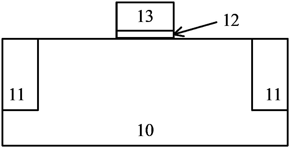
[0021] The present invention provides a method for manufacturing a semiconductor device, in particular to a method for manufacturing a transistor with epitaxial source and drain regions. For the manufacturing process, please refer to the appended Figure 2-11 .

[0022] First, see attached figure 2 , forming an STI (Shallow trench isolation, shallow trench isolation) structure 11 on the semiconductor substrate 10, and performing well region implantation. A semiconductor substrate 10 is provided. In this embodiment, a single crystal silicon substrate is ...


PUM


Abstract

The invention provides a method for manufacturing a semiconductor device having epitaxial source-drain areas. Epitaxial layers with the same impurities as traps are grown by an epitaxial way at source-drain grooves and are used as protection layers, so that CMOS device collusion can be prevented and thus the HALO effect can be replaced completely or partially; and then epitaxy of the source-drain areas can be carried out. Therefore, the performance and stability of the semiconductor device can be enhanced.

Description

technical field [0001] The invention relates to the field of manufacturing methods of semiconductor devices, in particular, to a method for manufacturing transistors with epitaxial source and drain regions. Background technique [0002] After semiconductor integrated circuit technology enters the technology node of 90nm feature size, it becomes more and more challenging to maintain or improve transistor performance. In the current mainstream technology, for PMOS, people use the method of epitaxially growing silicon germanium after forming trenches in the source and drain regions to provide compressive stress to squeeze the channel region of the transistor, thereby improving the performance of PMOS. At the same time, for NMOS, in order to achieve the same purpose, the method of epitaxial silicon carbon in the source and drain regions is also gradually adopted. See attached figure 1 , the figure is a schematic diagram of the structure of an existing transistor with epitaxial...

Claims


Application Information

Patent Timeline
IPC IPC(8): H01L21/336
Inventor 秦长亮殷华湘
Owner INST OF MICROELECTRONICS CHINESE ACAD OF SCI
Why Eureka
Try Eureka