
Operational transconductance amplifier with enhanced current sinking capacity

A current absorption and amplifier circuit technology, applied in the direction of DC coupled DC amplifiers, amplifiers with semiconductor devices/discharge tubes, amplifiers, etc., can solve the problems of insufficient absorption capacity of the current source 134, threat circuit, voltage rise, etc.

Active Publication Date: 2013-12-04
STMICROELECTRONICS (SHENZHEN) R&D CO LTD
View PDF8 Cites 0 Cited by
  • Summary
  • Abstract
  • Description
  • Claims
  • Application Information

AI Technical Summary

Problems solved by technology

There is a danger that the sinking capability of the current source 134 will be insufficient, which will cause an undesired voltage rise at the output node 140
A voltage rise at output node 140 may threaten downstream (eg, next stage) circuitry coupled to the output node

Method used


Image

  • Operational transconductance amplifier with enhanced current sinking capacity
  • Operational transconductance amplifier with enhanced current sinking capacity
  • Operational transconductance amplifier with enhanced current sinking capacity

Examples


Embodiment Construction

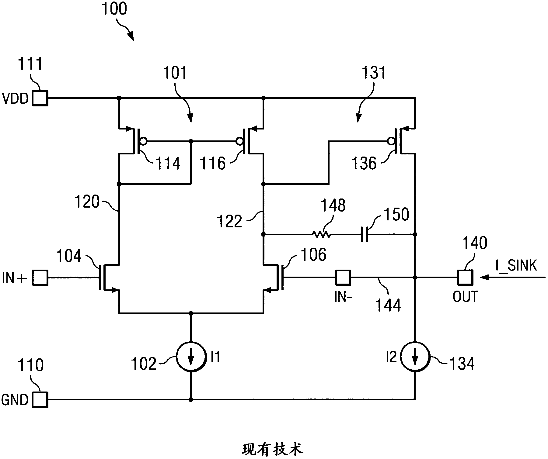
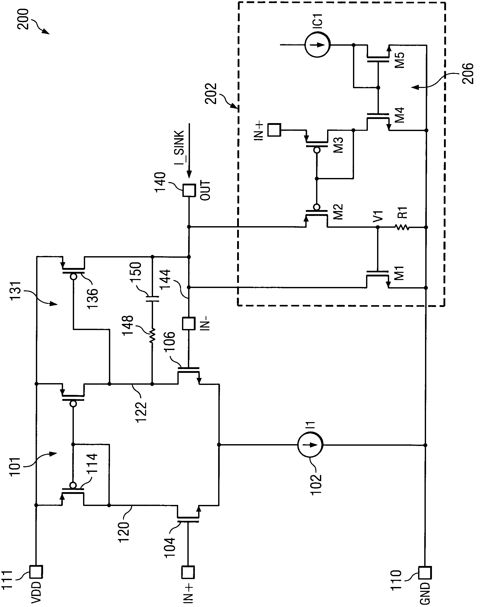
[0018] Now refer to figure 2 , which shows a circuit diagram of an operational transconductance amplifier 200 with enhanced current sinking capability.

[0019] figure 2 Like reference numerals refer to figure 1 Similar parts shown. I won't repeat it here figure 2 in such components, instead refer to the previously referenced figure 1 The description provided.

[0020] The difference between the amplifier 200 and the amplifier 100 is that the second current source 134 has been replaced by the current sink circuit 202 . The current sink circuit 202 includes a reference current source IC1 coupled to source current into a current mirror circuit 206 formed by transistors M4 and M5. Transistors M4 and M5 are n-channel type MOSFET transistors. The source terminals of transistors M4 and M5 are coupled to reference node 110 . The drain terminal of transistor M5 is coupled to receive the current sourced by reference current source IC1. The gate terminals of transistors M4 a...


PUM


Abstract

An embodiment of the invention provides an operational transconductance amplifier with the enhanced current sinking capacity. An amplifier circuit comprises an input terminal and an output terminal. A current sinking transistor comprises a first conductive terminal coupled to the output terminal and a second conductive terminal coupled to a reference power supply node. A voltage sensing circuit comprises a first input coupled to the input terminal and a second input coupled to the output terminal. The output of the voltage sensing circuit is coupled to a control terminal of the current sinking transistor. The voltage sensing circuit is used for sensing rise of the voltage of the output terminal, which exceeds the voltage of the input terminal, and responding to the rise by activating the current sinking transistor.

Description

technical field [0001] The present invention relates generally to amplifier circuits, and in particular to operational transconductance amplifier circuits. Background technique [0002] refer to figure 1 , shows a circuit diagram of a conventional operational transconductance amplifier 100 configured as a non-inverting unity-gain buffer. [0003] Amplifier 100 includes a differential input stage 101 including a first current source 102 as a tail current source for differential transistor pair 104 and 106 . Transistors 104 and 106 comprise MOSFET transistors of the n-channel type, the source terminals of transistors 104 and 106 being connected together at node 108 . A first current source 102 is coupled between node 108 and a reference node 110 (including circuit ground GND in the illustrated circuit). The gate of transistor 104 is coupled to the positive input terminal IN+ of amplifier 100 . The gate of transistor 106 is coupled to the negative input terminal IN− of ampl...

Claims


Application Information

Patent Timeline
IPC IPC(8): H03F3/45
CPCH03F3/45183H02H9/043H03F3/45071H03F2203/45526H03F2203/45674H03F3/45179H03F2200/471H03F2203/45022
Inventor 段毅君
Owner STMICROELECTRONICS (SHENZHEN) R&D CO LTD
Features
  • Generate Ideas
  • Intellectual Property
  • Life Sciences
  • Materials
  • Tech Scout
  • Unparalleled Data Quality
  • Higher Quality Content
  • 60% Fewer Hallucinations
Learn More