Image sampling circuit with a blank reference combined with the video input

a blank reference and video input technology, applied in the field of analog frontends for imaging sensors, can solve the problem that traditional operational amplifiers cannot accommodate a wide bandwidth, and achieve the effect of improving the signal to noise ratio, without adversely affecting the bandwidth

Active Publication Date: 2005-10-04
EXAR CORP
View PDF16 Cites 28 Cited by
  • Summary
  • Abstract
  • Description
  • Claims
  • Application Information

AI Technical Summary

Benefits of technology

[0011]The use of a transconductance amplifier provides the ability to improve the signal to noise ratio by maximizing the ratio of the signal current to the constant bias current, within the constraints of allowable power dissipation. This amplifier is not limited by the supply voltage, as are prior art voltage amplifiers. In addition, the combination of a transconductance and trans impedance amplifier allows the gain to be changed without adversely affecting the bandwidth. Traditional operational amplifiers cannot accommodate a wide bandwidth over a significantly changing range of gains.
[0012]One embodiment of the invention also provides for both coarse and fine offset adjustment, by providing both pre- and post-gain offset adjustments. In the AFE embodiment, the coarse offset is provided in the black reference level sampler, and the fine offset is provided in the programmable switched capacitor amplifier. The voltage reference of the black reference sampler is two separate voltage references. Each of these voltage references can be independently programmed through a digital-to-analog converter (DAC) input from the external digital processing circuitry. This thus allows pre-gain offset correction to be combined with the black reference signal.
[0014]In yet another embodiment, the invention implements a piece-wise linear approximation of an exponential gain function. The transconductance and transimpedance amplifiers are programmed to provide exponential jumps in gain, while the switched capacitor amplifier is programmed to interpolate as needed between the gain levels of the transconductance and transimpedance amplifiers. The selection circuitry and resistor values are chosen to enable an even multiple of the gain to be selected by changing only certain most significant bits (MSBs) of the gain control register, simplifying user programmability.

Problems solved by technology

Traditional operational amplifiers cannot accommodate a wide bandwidth over a significantly changing range of gains.

Method used


Image

  • Image sampling circuit with a blank reference combined with the video input
  • Image sampling circuit with a blank reference combined with the video input
  • Image sampling circuit with a blank reference combined with the video input

Examples


Embodiment Construction

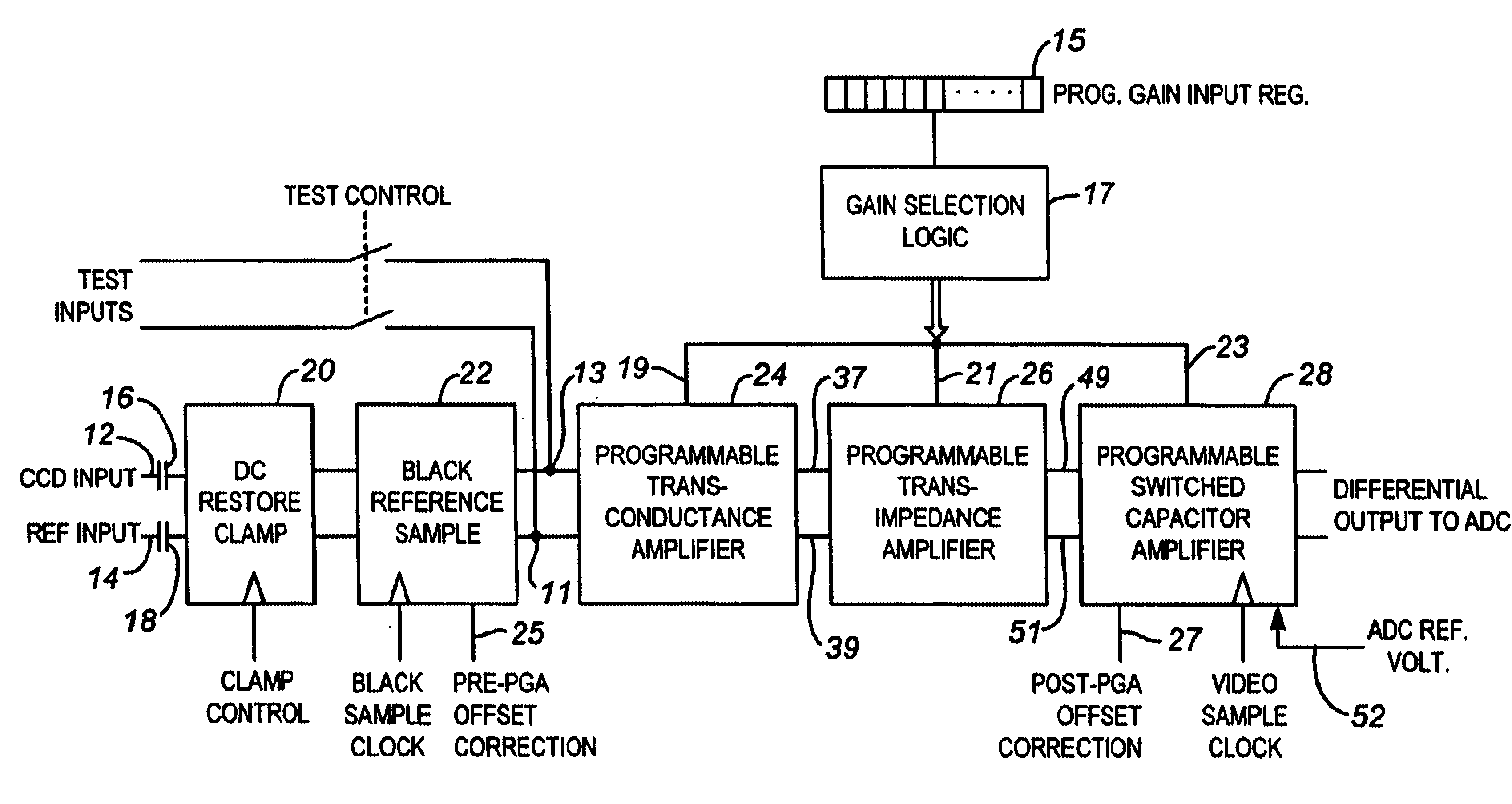
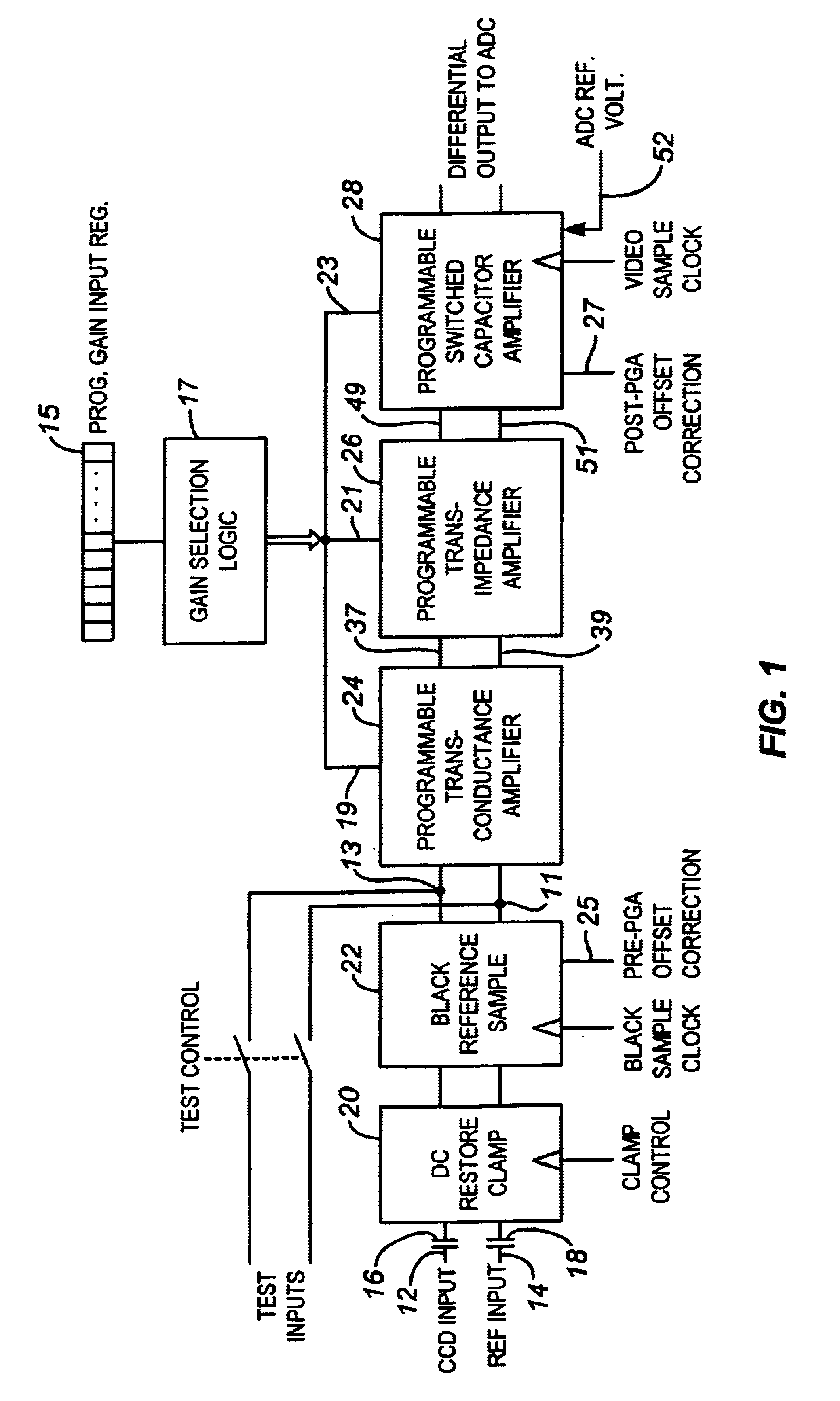
[0027]FIG. 1 illustrates an AFE according to the invention. A CCD input is provided on a line 12, with a reference input being provided on a line 14. These are connected through external capacitors 16 and 18, respectively, to a DC restore clamp 20. The output of DC restore clamp 20 is provided to a black reference sampler circuit 22 according to this invention.

[0028]The output of the black reference sampler circuit is provided to a programmable transconductance amplifier 24, which is coupled to a programmable transimpedance amplifier 26, which in turn is coupled to a programmable switched capacitor amplifier 28. The AFE is designed to convert the CCD output signal into a corrected signal for an analog-to-digital converter (ADC) by performing gain, offset correction and elimination of pixel-to-pixel variations.

[0029]The gain is programmed by a value input by a user to a programmable gain input register 15. This value is provided to gain selection logic 17, which determines the approp...


PUM


Abstract

A programmable gain amplifier having three separately programmable amplifiers. A programmable transconductance amplifier is followed by a programmable transimpedance amplifier, then a programmable switched capacitor amplifier. In one embodiment, this programmable gain amplifier is implemented in an analog front-end (AFE) circuit. One AFE embodiment provides a coarse pre-gain offset a black reference level sampler, and a fine post-gain offset in the programmable switched capacitor amplifier. In one embodiment, an ADC reference is sampled, and is subtracted directly from the video signal in the switched capacitor amplifier so that the zero level of the video signal is made to correspond to the zero level of the ADC. In another embodiment, a piece-wise linear approximation of an exponential gain function is implemented by programming the transconductance and transimpedance amplifiers to provide exponential jumps in gain, while the switched capacitor amplifier is programmed to interpolate as needed between the exponential gain levels.

Description

BACKGROUND OF THE INVENTION[0001]The present invention relates to an analog front-end (AFE) for an imaging sensor, and in particular to a correlated double sampler (CDS), programmable gain amplifier (PGA), and sample and hold circuit (S / H) for CCD signal digitization.[0002]Imaging systems which may support a CCD sensor or a CMOS sensor typically require an AFE chip which samples the analog signal under control of a timing generator. Typically, a voltage amplifier is used. The sampled signal is then amplified and provided to a separate chip for digitization and subsequent processing.[0003]Typically, a black reference level is sampled immediately before every pixel of a video signal. These two values are then separately provided to the digital processing circuitry. Related prior art is described below:[0004]U.S. Pat. No. 5,796,361. This patent describes a single chip, cost effective implementation of a CCD signal digitizing circuit which uses a standard technique to correct for the pi...

Claims


Application Information

Patent Timeline
Patent Type & Authority Patents(United States)
IPC IPC(8): H03F3/00H03F3/45H04N5/16H04N5/20H04N5/217H04N5/361H04N5/378
CPCH03F3/005H03F3/45197H04N5/16H04N5/20H04N5/2176H03F2203/45504H03F2203/45616H03F2203/45726H04N25/63
Inventor GOWER, RICHARD L.HOFFMAN, ERIC G.AHUJA, BHUPENDRA K.SALCEDO, J. ANTONIO
Owner EXAR CORP
Why Eureka
Try Eureka