
Systems and methods for programming large-scale field-programmable analog arrays

a field-programmable analog array and programming system technology, applied in the field of field-programmable field-programmable analog arrays, can solve the problems of limited functionality and flexibility, long development cycle of analog processing and storage circuits, and limited usefulness and versatility of current fpaas, and achieve the effect of greater flexibility

Active Publication Date: 2006-11-23
GEORGIA TECH RES CORP
View PDF11 Cites 29 Cited by
  • Summary
  • Abstract
  • Description
  • Claims
  • Application Information

AI Technical Summary

Benefits of technology

[0015] A notable feature of the present invention is the use of the transistors in the floating-gate transistor array as both switching elements for routing signals and as programmable elements for manipulating the signal being routed. By using the transistors as multi-purpose elements, greater flexibility may be achieved in implementing designs using the present invention.

Problems solved by technology

Currently, circuits used for analog processing and storage have a long development cycle and are typically large.
Unfortunately, each of these alternatives trade area for improved switch characteristics and require an additional physical memory element for maintaining connectivity within the FPAA.
FPAAs have been of interest for some time, but historically, these devices have had very few programmable elements and limited interconnect capabilities, making them limited in their usefulness and versatility.
While specific architectures vary, their small sized and often restrictive interconnect designs leave current FPAAs limited in functionality and flexibility.
Unfortunately, a problem looms on the horizon: the power consumption of the ADC does not follow Gene's law and will soon dominate the total power budget of digital systems.
While ADC resolution has been increasing at roughly 1.5 bits every five years, the power performance has remained the same, and soon, physical limits will further slow progress.
This is a power intensive approach and makes use of certain communication schemes impractical in portable applications.
The front-end analog-to-digital converter and back-end digital-to-analog converter required in these systems become expensive when the signal is of a wideband nature and high resolution is desired.
Unfortunately, no such analog waveform generator exists.

Method used


Image

  • Systems and methods for programming large-scale field-programmable analog arrays
  • Systems and methods for programming large-scale field-programmable analog arrays
  • Systems and methods for programming large-scale field-programmable analog arrays

Examples


Embodiment Construction

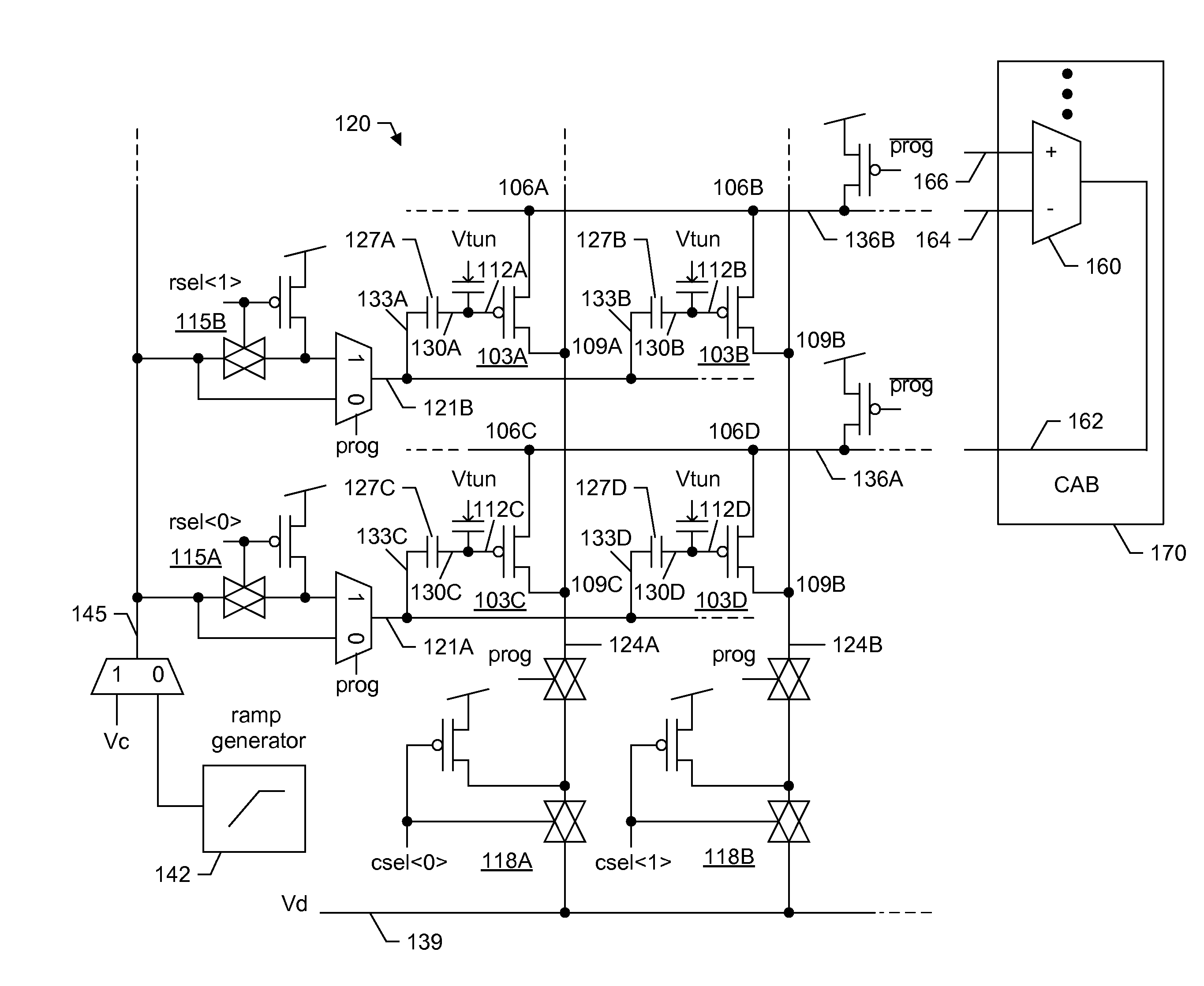
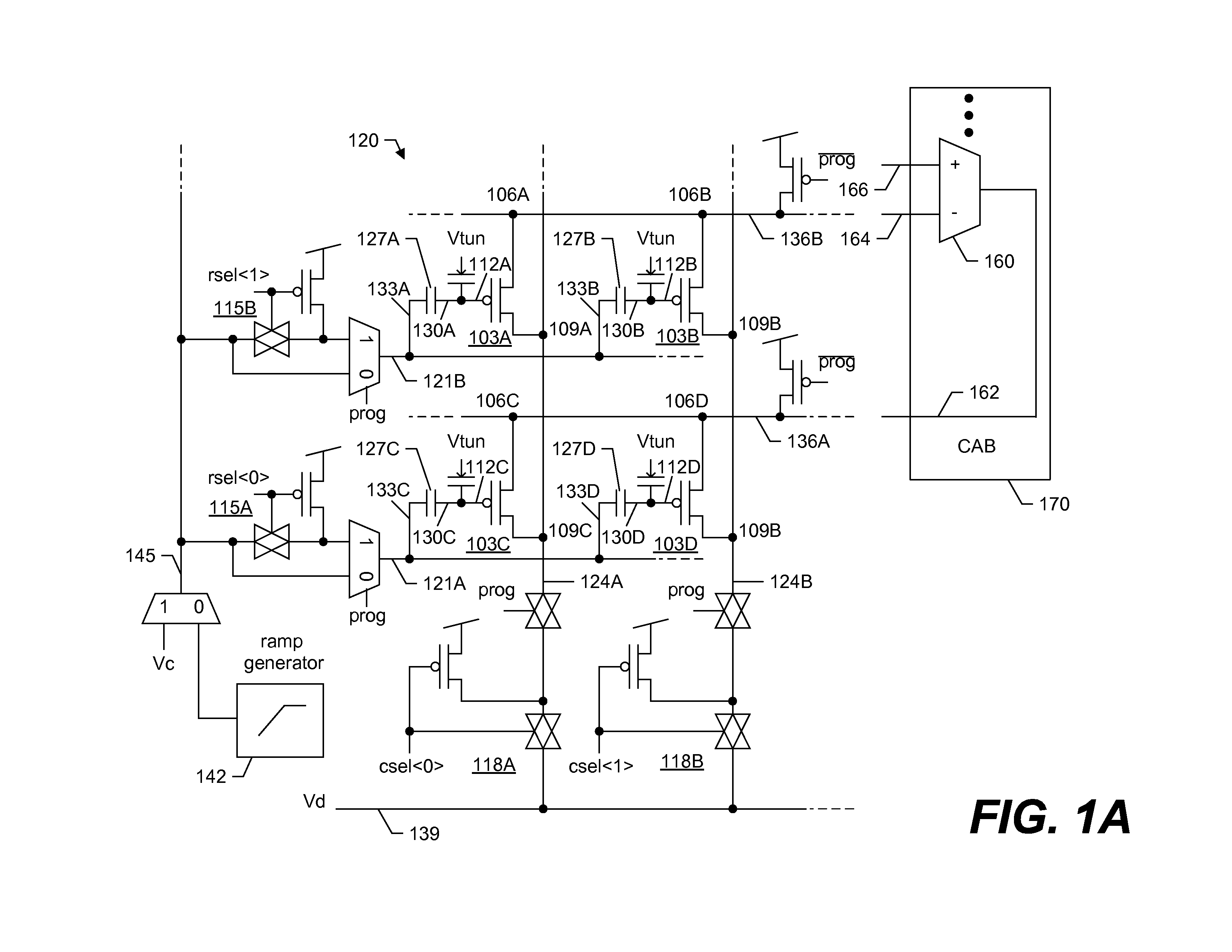
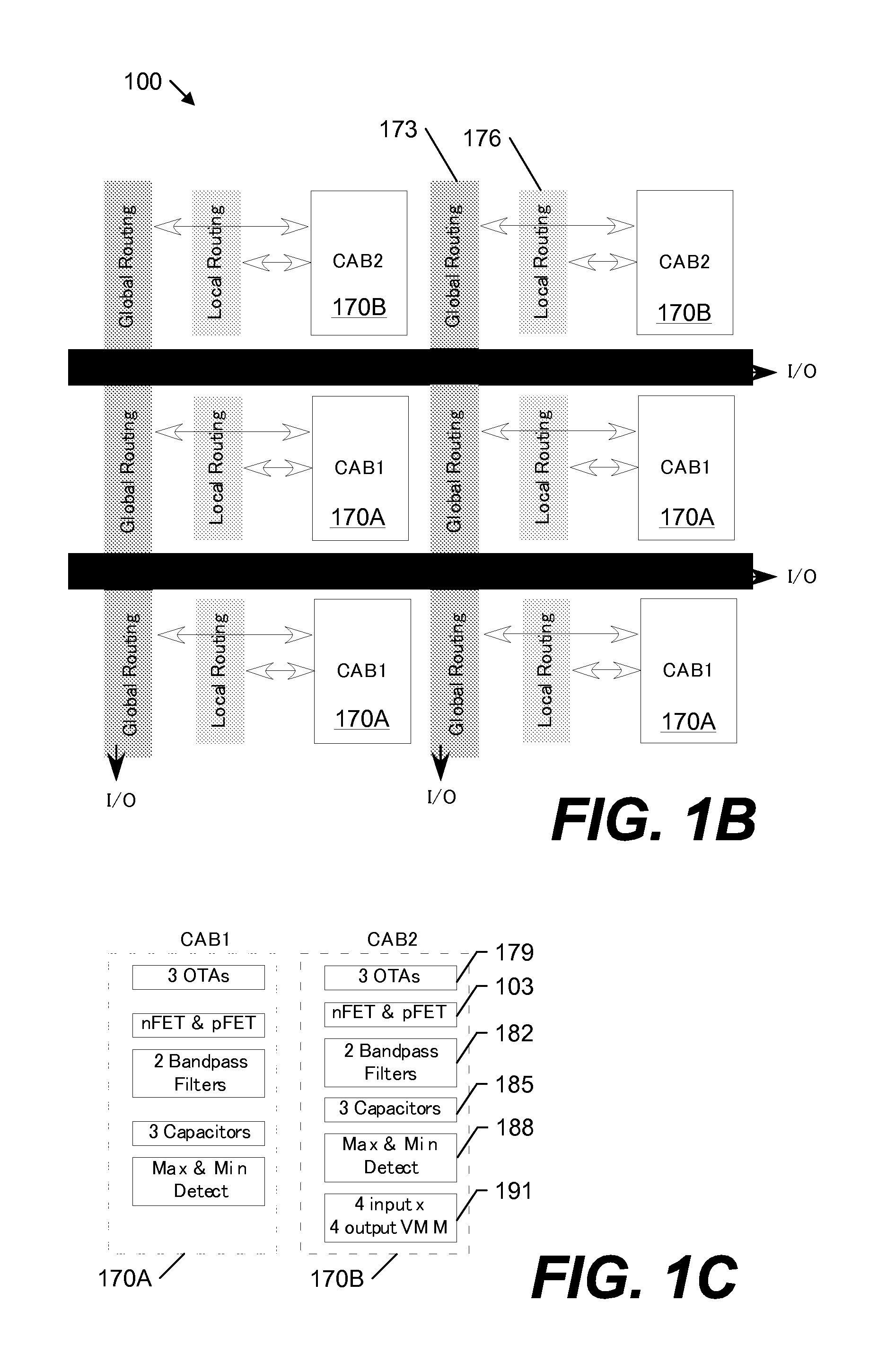
[0045] Referring now in detail to the drawing figures, wherein like reference numerals represent like parts throughout the several views, FIG. 1 illustrates a large-scale field-programmable analog array (FPAA) 100 utilizing computational analog blocks (CAB) 170 and floating-gate switches 103 in accordance with an exemplary embodiment of the present invention. Traditionally, FPAAs are distinguished from one another by two basic components: a computational analog block (CAB) 170, and an interconnect network. A conventional FPAA's interconnect structure is most commonly connected by MOS transistor switches driven by digital memory. If T-gates are not introduced, the range of passable signals within an FPAA is dramatically smaller than the range of the power supply, because of the non-linear resistance of the MOSFET. Accordingly, in most conventional FPAAs, T-gate switches are introduced, thereby requiring additional space and potentially introducing parasitics. Although alternatives to...


PUM


Abstract

A large-scale field-programmable analog array (FPAA) for rapidly prototyping analog systems and an arbitrary analog waveform generator. The large-scale FPAA includes a floating-gate transistor array and a plurality of computational analog blocks (CABs), which may be adapted to set bias voltages for operational transconductance amplifiers (OTAs), adjust corner frequencies on the capacitively coupled current conveyors, set multiplier coefficients in vector-matrix multipliers, and a variety of other operations. The floating-gate transistors may be used as switch elements, programmable resistor elements, precision current sources, and programmable transistors. Accordingly, the floating-gate transistors within the array allow on-chip programming of the characteristics of the computational elements, while still maintaining compact CABs. The arbitrary analog waveform generator may include programmable floating-gate MOS transistors for use as analog memory cells to store samples of the waveforms.

Description

CROSS REFERENCE TO RELATED APPLICATIONS [0001] This application is a continuation-in-part of U.S. patent application Ser. No. 11 / 382,640, filed on 10 May 2006, the entire contents of which are hereby incorporated by reference. This application also claims priority of U.S. Provisional Patent Application No. 60 / 681,715, filed 16 May 2005, and U.S. Provisional Patent Application No. 60 / 686,559, filed 02 Jun. 2005, the entire contents of which are hereby incorporated by reference.BACKGROUND [0002] 1. Field of the Invention [0003] The present invention relates to field-programmable analog arrays and, more particularly, to programming large-scale field-programmable analog arrays for use in analog circuitry. [0004] 2. Description of Related Art [0005] Even in today's world of digital electronics, it is often desirable, or even necessary to use and process analog signals. For example, most audio files, while typically stored in digital form such as MP3s and compact disks, must be converted ...

Claims


Application Information

Patent Timeline
Patent Type & Authority Applications(United States)
IPC IPC(8): H03K19/173
CPCH03K19/17732H03K19/173
Inventor TWIGG, CHRISTOPHER M.HASLER, PAUL E.GRAY, JORDAN D.CHAWLA, RAVI
Owner GEORGIA TECH RES CORP
Learn More