Method for manufacturing pad for touch panel, and pad for touch panel manufactured by method
A technology of touch panel and manufacturing method, applied in the direction of printed circuit manufacturing, input/output process of data processing, conductive layer on insulating carrier, etc., to achieve the effect of simplifying procedures and reagents, and reducing wiring short circuit
- Summary
- Abstract
- Description
- Claims
- Application Information
AI Technical Summary
Problems solved by technology
Method used
Image
Examples
Embodiment Construction
[0044]Embodiments of the present invention will be described in detail below with reference to the accompanying drawings so that those skilled in the art to which the present invention pertains can easily implement. However, the present invention can be embodied in various forms, and is not limited to the embodiments described here. In addition, in the drawings, parts irrelevant to the description are omitted in order to clarify the present invention, and similar reference numerals are assigned to similar parts throughout the specification.
[0045] Throughout the specification, when it is stated that a certain part "includes" a certain technical feature, unless there is no specific contrary statement, this does not mean excluding other technical features, but means that other technical features can be further included.
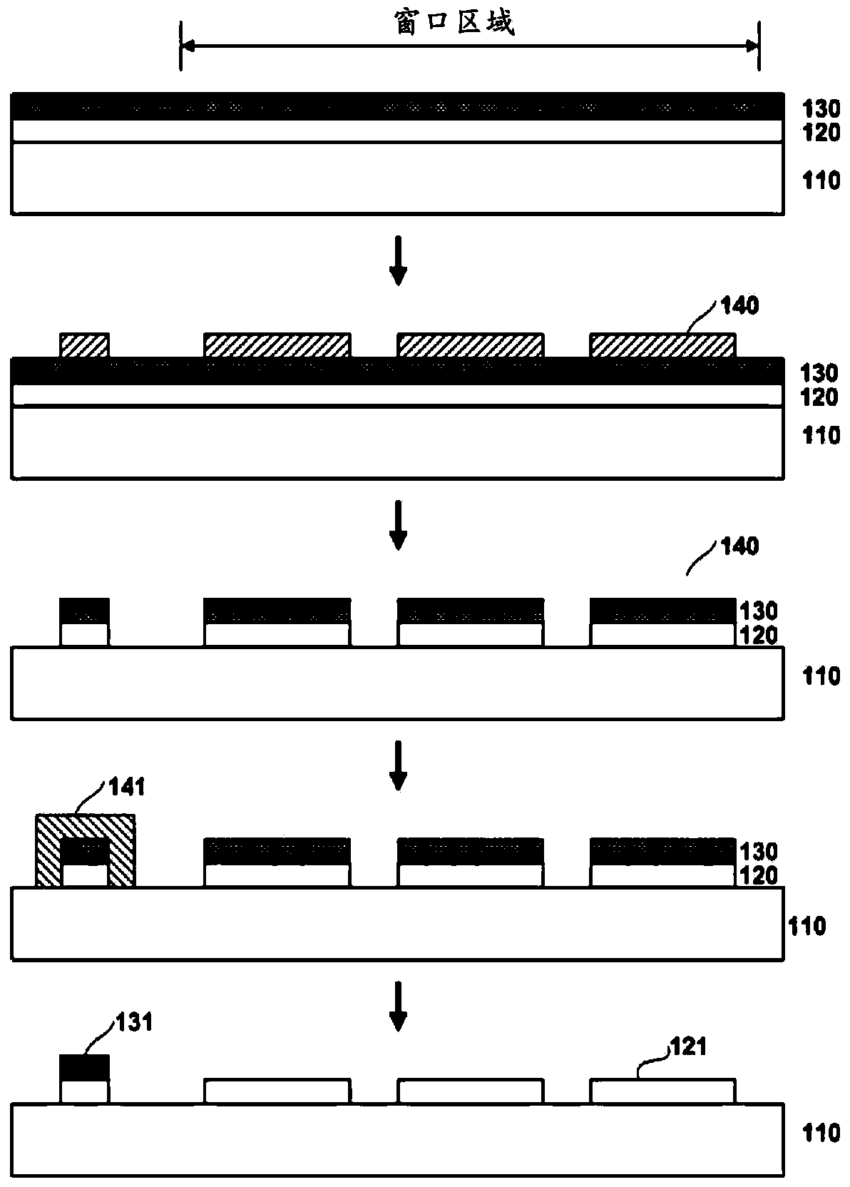
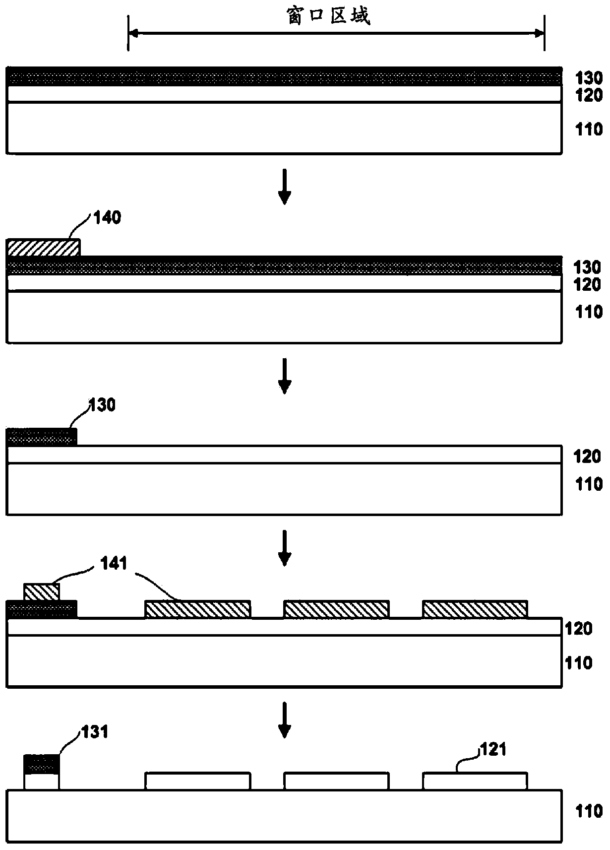
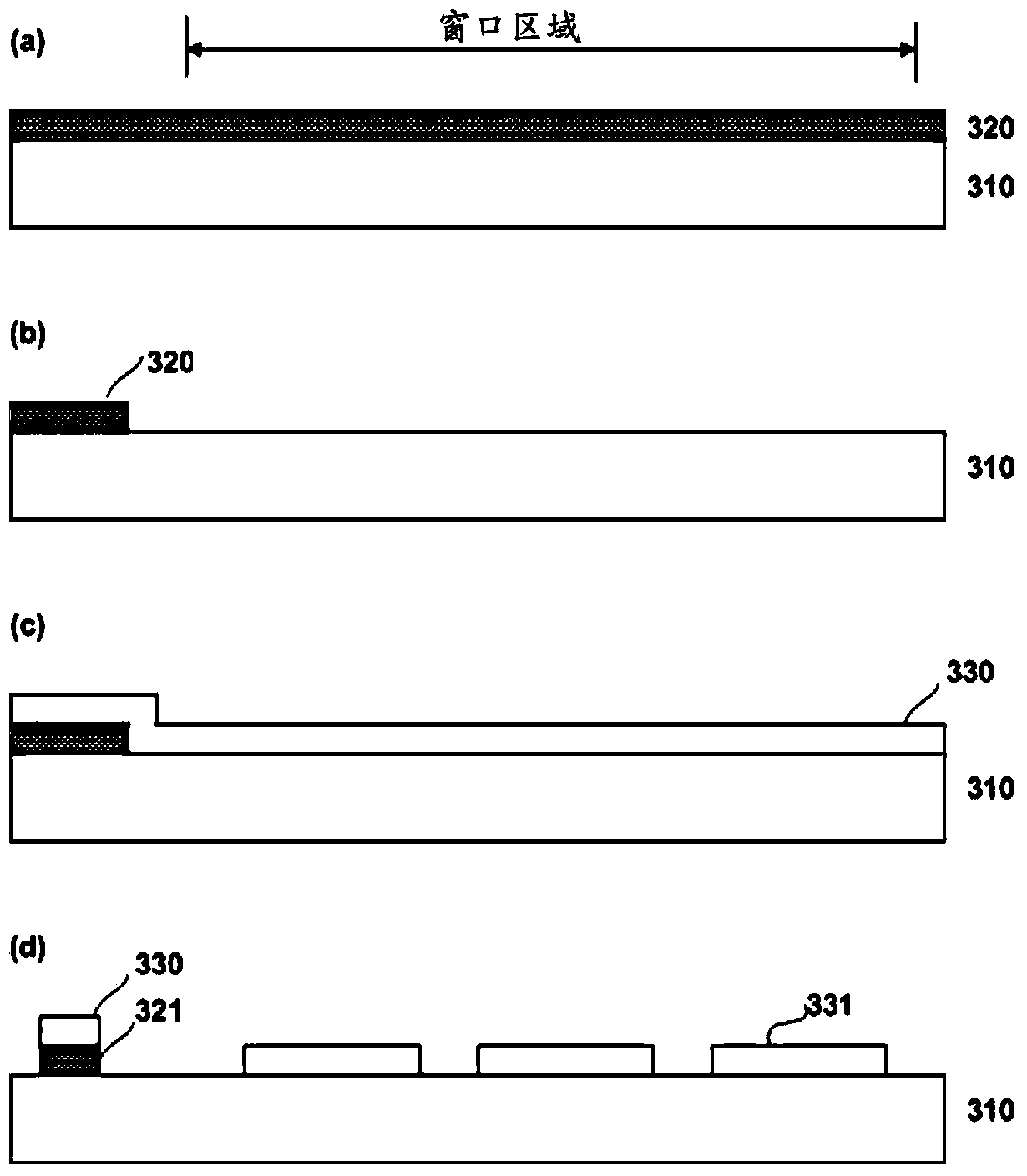
[0046] image 3 is a cross-sectional view showing step by step a method of manufacturing a backing plate for a touch panel according to an embodiment of the...
PUM
 Abstract
Description
Claims
Application Information


