Chip and method for debugging MCU through I2C slave unit

A technology of chips and devices, which is applied in the field of debugging MCU chips from devices through I2C, can solve problems such as wasting system resources, and achieve the effect of saving resources.

Active Publication Date: 2013-12-11
SHENZHEN HANGSHUN CHIP TECH DEV CO LTD
View PDF6 Cites 21 Cited by
  • Summary
  • Abstract
  • Description
  • Claims
  • Application Information

AI Technical Summary

Problems solved by technology

The communication and debugging between the chip and the MCU mainly use JTAG, UART and other methods, so when the chip does not integrate JTAG, UART and other interfaces, it is necessary to add additional interfaces for debugging, wasting system resources

Method used


Image

  • Chip and method for debugging MCU through I2C slave unit
  • Chip and method for debugging MCU through I2C slave unit
  • Chip and method for debugging MCU through I2C slave unit

Examples


Embodiment 1

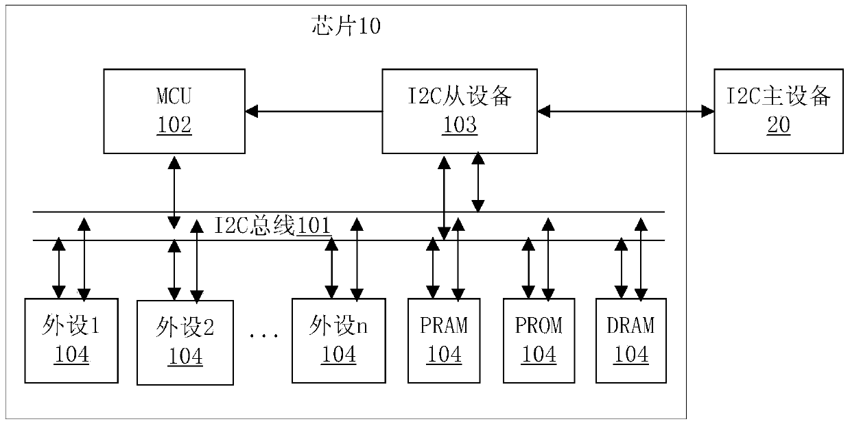
[0045] figure 1 It is a control schematic diagram of a chip debugging MCU provided by an I2C slave device provided by an embodiment of the present invention. The system includes a chip 10 and an I2C master device 20, wherein:

[0046] The chip 10 includes an I2C bus 101 , an MCU 102 , an I2C slave 103 and more than two peripherals 104 . The MCU 102 , the I2C slave device 103 and the peripheral device 104 are connected through the I2C bus 101 .

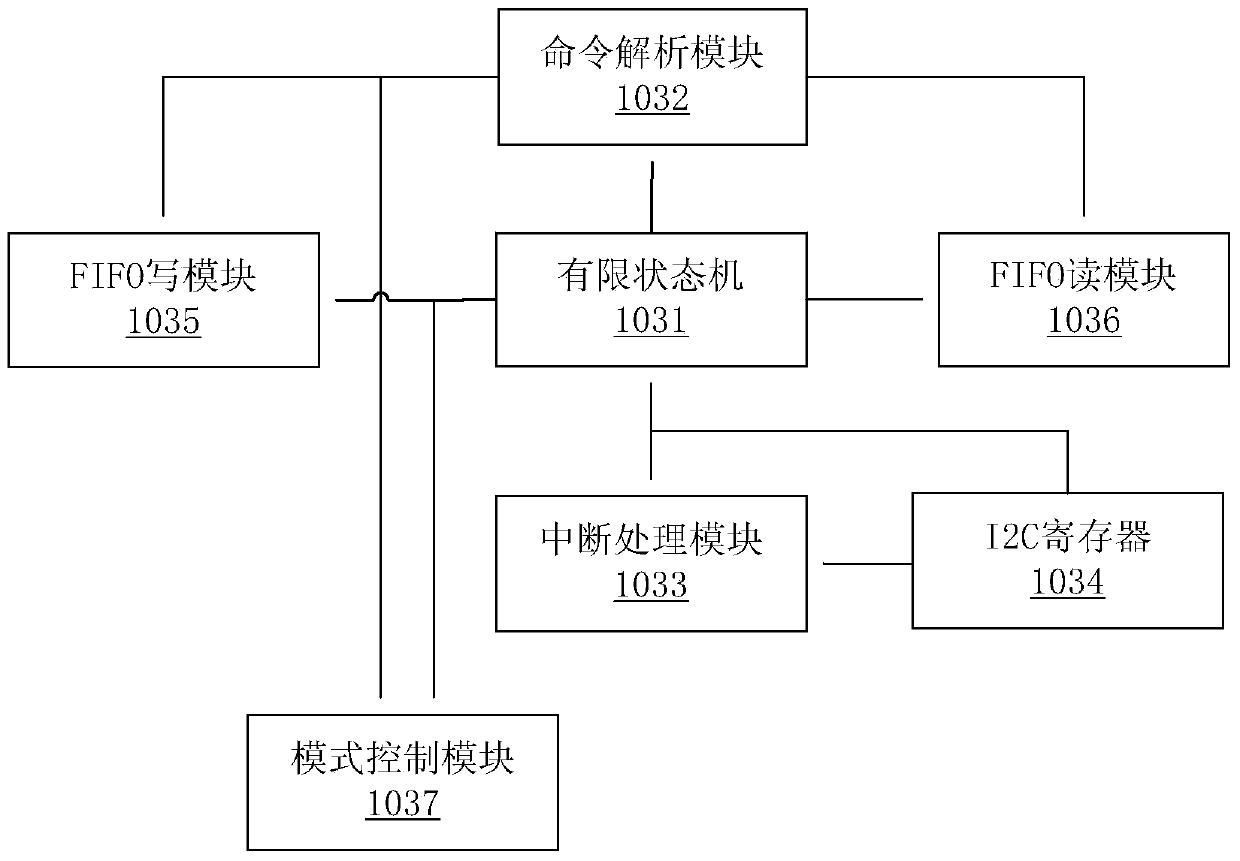
[0047]Wherein, the I2C bus 101 and the MCU102 belong to the prior art, and the I2C slave device 103 can also be used as a debugging interface except for maintaining the existing general data transmission interface function, and enter or exit the debugging MCU under the control of the I2C master device 20 outside the chip mode, so as to achieve the selection of general data transmission interface or debugging interface. Peripherals 104 are also present including, but not limited to, read registers, write registers, program memory, and...


PUM


Abstract

The invention discloses a chip and method for debugging an MCU through an I2C slave unit, and belongs to the technical field of electronic circuits. The chip comprises an I2C bus, the MCU, the I2C slave unit and more than two peripherals, wherein the MCU, the I2C slave unit and the peripherals are connected through the I2C bus; the I2C slave unit is also used for being controlled by an I2C master device outside the chip to enter or quit an MCU debugging mode. By adopting the embodiment of the chip and method for debugging the MCU through the I2C slave unit, under the condition that general functions of the I2C slave unit are not affected, the chip also can serve as a debugging interface, therefore, a debugging function can be achieved without additionally adding other debugging interfaces, and resource consumption is reduced.

Description

technical field [0001] The invention relates to the technical field of electronic circuits, in particular to a chip and a method for debugging an MCU through an I2C slave device. Background technique [0002] In traditional chip systems, I2C slave devices are usually used as a general data transmission interface. The communication and debugging between the chip and the MCU mainly use JTAG, UART, etc., so when the chip does not integrate JTAG, UART and other interfaces, it is necessary to add an additional interface for debugging, wasting system resources. Contents of the invention [0003] In view of this, the technical problem to be solved by the present invention is to provide a chip and method for debugging the MCU through the I2C slave device, so that the I2C slave device can stop and release the MCU at any time, and can perform a handshake operation with the program executed by the MCU. Use the I2C slave device to realize the debugging function of the peripheral to t...

Claims


Application Information

Patent Timeline
Patent Type & Authority Applications(China)
IPC IPC(8): G06F13/38G06F11/36
CPCG06F11/3648
Inventor 郭正伟王光耀
Owner SHENZHEN HANGSHUN CHIP TECH DEV CO LTD
Why Eureka
Try Eureka