Chip physical integrity detecting device

A technology of integrity detection and detection devices, applied in the direction of platform integrity maintenance, etc., to achieve the effects of expanding coverage, reducing power consumption, and reducing area

Active Publication Date: 2013-12-11
DATANG MICROELECTRONICS TECH CO LTD
View PDF3 Cites 10 Cited by
  • Summary
  • Abstract
  • Description
  • Claims
  • Application Information

AI Technical Summary

Problems solved by technology

[0014] The technical problem to be solved by the present invention is to propose a chip physical integrity detection device to redu

Method used


Image

  • Chip physical integrity detecting device
  • Chip physical integrity detecting device
  • Chip physical integrity detecting device

Examples


Embodiment 1

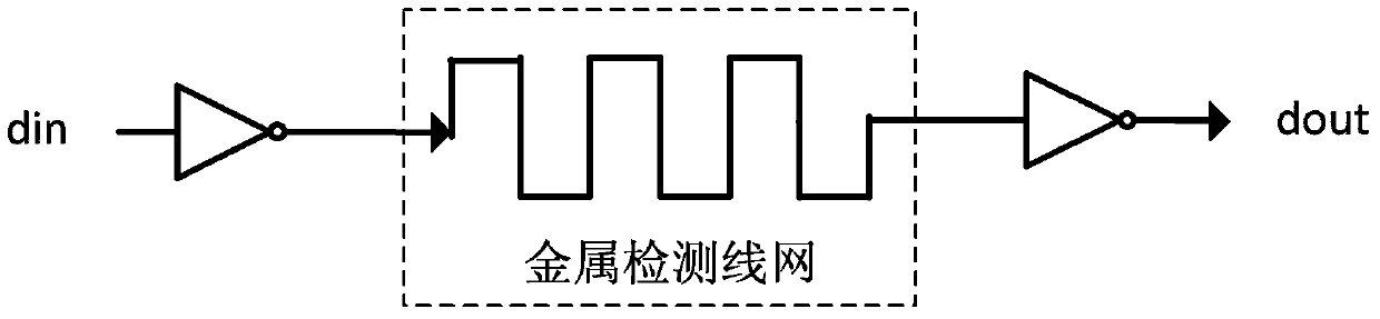
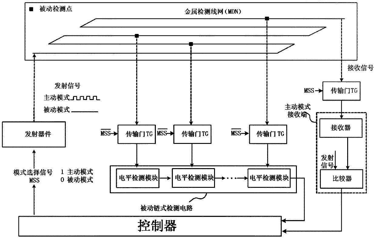
[0059] Active detection mode (Active Shield)

[0060] When the mode selection signal sent by the controller is 1, the active detection mode starts and the passive detection mode stops.

[0061] The transmission gate TG connected to the receiver is opened, and the transmission gate TG connected to the level detection module is closed.

[0062] Active detection mode includes the following 4 parts: transmitter, metal detection network, receiver, and comparator.

[0063] The emission signal generated by the transmitter when the active detection mode is valid is a square wave signal with an unfixed period. The emission signal corresponds to the metal detection network. For example, if the chip has 32 metal detection network, there are 32 detection signals. The waveform and phase of the signals are different.

[0064] The receiver receives the receiving signal from the metal detection network.

[0065] The comparator compares the transmitted signal and the received signal. If the two wavefor...

Embodiment 2

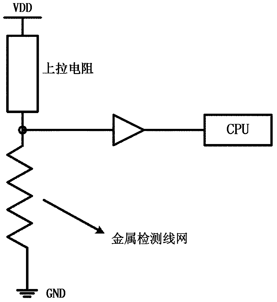
[0067] Passive detection mode (Passive Shield)

[0068] When the mode selection signal sent by the controller is 0, the passive detection mode starts and the active detection mode stops. The transmission gate circuit TG connected to the level detection module is opened, and the transmission gate circuit TG connected to the receiving device is closed.

[0069] The detection input end of the level detection module is connected to the detection point of the metal detection wire net, and the level detection module can detect whether the potential of the detection point is normal or floating. If the potential of the detection point is floating, an abnormal value is output.

[0070] If the front-end input of the level detection module is an abnormal value, the abnormal value is output.

[0071] The level detection module is composed of digital standard units. The detection frequency of the level detection module is controlled by the detection frequency control signal.

[0072] Such as Fig...


PUM


Abstract

The invention discloses a chip physical integrity detecting device and belongs to the field of chip physical integrity detection. The chip physical integrity detecting device comprises a controller, a transmitter, a metal detection net and a detector, wherein the controller is used for selecting detection modes and emitting mode selection signals according to the working state of a chip to be detected, the controller is also used for judging whether the chip to be detected is abnormal according to potential information fed back by the detector, the transmitter is used for transmitting signals to the metal detection net according to the mode selection signals, and the detector is used for detecting potential information of a signal end of the metal detection net connected with the detector according to the mode selection signals and sending the detected potential information to the controller. According to the chip physical integrity detecting device, due to the fact that work in carried out by means of switching between two detection modes, the detachable destroy behavior coverage can be enlarged; compared with a device only using an active detection mode always, the chip physical integrity detecting device has the advantage of being capable of reducing power consumption remarkably.

Description

Technical field [0001] The invention relates to the field of chip physical integrity detection. Background technique [0002] Intrusive attacks on chips, also known as physical attacks, refer to the information spying and malicious destruction carried out by the attackers through physical means (such as with special equipment). Including stripping, probes, focused ion beam FIB, etc. One of the solutions to physical attacks at this stage is top-level metal detection. When the chip is physically attacked, the top metal will be destroyed, and the detection device will detect that the top metal is damaged and send an alarm signal. [0003] The existing top-level metal detection generally adopts a passive detection method or an active detection method. figure 1 As shown, the passive detection method adopts a pull-up resistive detection method or a pull-down resistive detection method. The pull-up resistance detection method means that one end of the metal detection wire net is ground...

Claims


Application Information

Patent Timeline
IPC IPC(8): G06F21/50
Inventor 高洪福何其李军
Owner DATANG MICROELECTRONICS TECH CO LTD
Why Eureka
Try Eureka