Semiconductor device with air gap and method for fabricating the same
A technology of semiconductor and air gap, which is applied in the field of semiconductor devices with air gap and its manufacturing, and can solve problems such as low dielectric constant
- Summary
- Abstract
- Description
- Claims
- Application Information
AI Technical Summary
Problems solved by technology
Method used
Image

Examples
Embodiment Construction
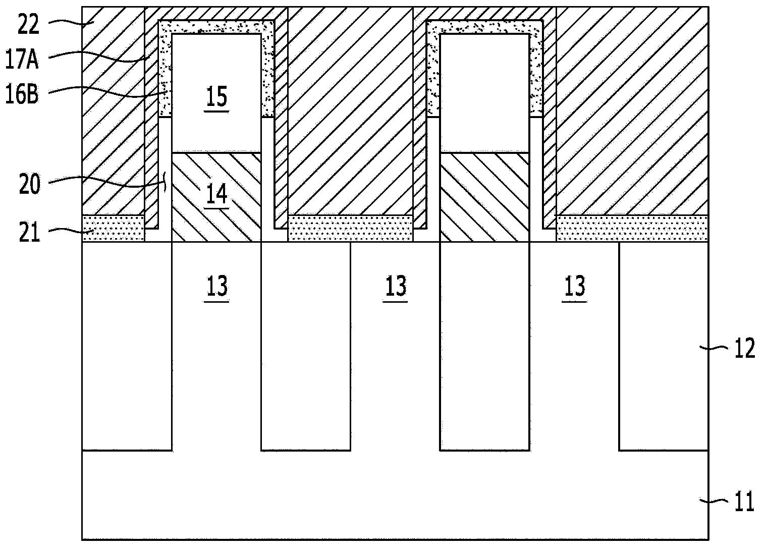
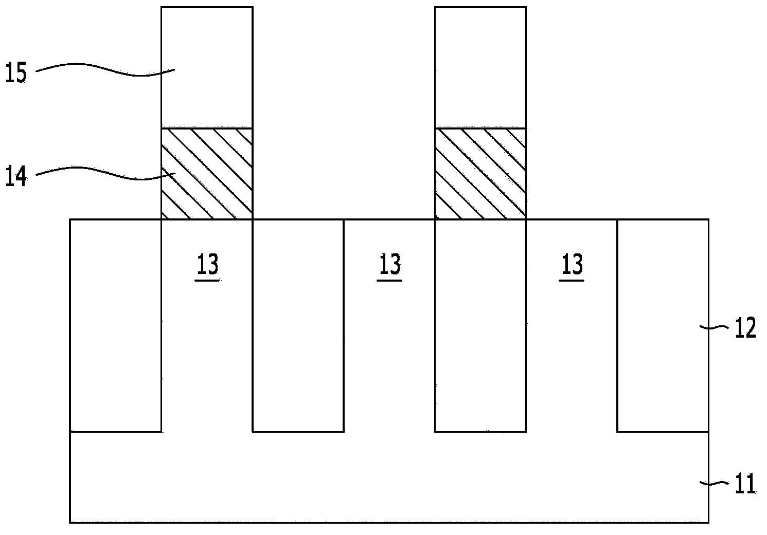
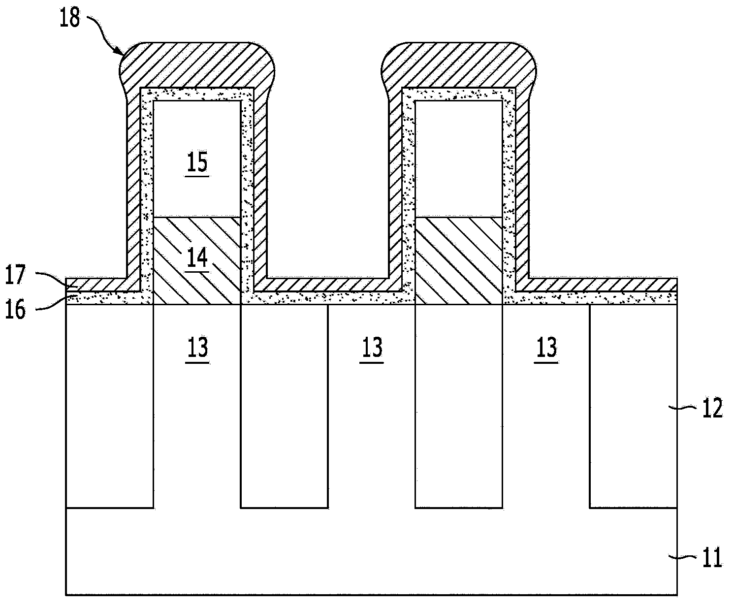
[0029] Exemplary embodiments of the present invention will be described in more detail below with reference to the accompanying drawings. However, this invention may be embodied in various forms and should not be construed as limited to the examples provided herein. Rather, these embodiments are provided so that this specification will be thorough and complete, and will fully convey the scope of the invention to those skilled in the art. In the specification, the same reference numerals refer to similar parts in different figures and embodiments of the invention.
[0030] The drawings are not to scale and in some instances proportions may have been exaggerated in order to clearly illustrate features of the embodiments. When referring to a first layer being "on" a second layer or "on" a substrate, it refers not only to the case where the first layer is formed directly on the second layer or on the substrate, but also to the case where the first layer is formed with the substra...
PUM
 Abstract
Description
Claims
Application Information
 - R&D
- Intellectual Property
- Life Sciences
- Materials
- Tech Scout
- Unparalleled Data Quality
- Higher Quality Content
- 60% Fewer Hallucinations
Browse by: Latest US Patents, China's latest patents, Technical Efficacy Thesaurus, Application Domain, Technology Topic, Popular Technical Reports.
© 2025 PatSnap. All rights reserved.Legal|Privacy policy|Modern Slavery Act Transparency Statement|Sitemap|About US| Contact US: help@patsnap.com