Multi-layer circuit board and manufacturing method thereof

A technology of a multilayer circuit board and a manufacturing method, which is applied in the direction of multilayer circuit manufacturing, printed circuit components, etc., can solve the problems of affecting the service life of the circuit board, the large difference in the expansion coefficient, and the low flatness of the base layer, so as to improve the The effect of long service life, smooth surface and short process time

Active Publication Date: 2013-12-18
QI DING TECHNOLOGY QINHUANGDAO CO LTD +1
View PDF3 Cites 3 Cited by
  • Summary
  • Abstract
  • Description
  • Claims
  • Application Information

AI Technical Summary

Problems solved by technology

However, the thermal expansion coefficient of the organic resin material is quite different from that of the chip made of silicon chip mounted on the conductive circuit, which will easily cause the conductive line between the base layer and the chip to break, thereby affecting the service life of the circuit board
In addition, due to the low flatness of the base layer made of organic resin materials, it is difficult to directly form precise and ultra-fine line patterns (ie L / S less than or equal to 10 / 10um) on the base layer

Method used


Image

  • Multi-layer circuit board and manufacturing method thereof
  • Multi-layer circuit board and manufacturing method thereof
  • Multi-layer circuit board and manufacturing method thereof

Examples


Embodiment Construction

[0029] The manufacturing method of the multilayer circuit board provided by the technical solution and the multilayer circuit board made by the method will be further described in detail below in conjunction with the drawings and embodiments.

[0030] The manufacturing method of the multilayer circuit board provided by the first embodiment of the technical solution includes the following steps:

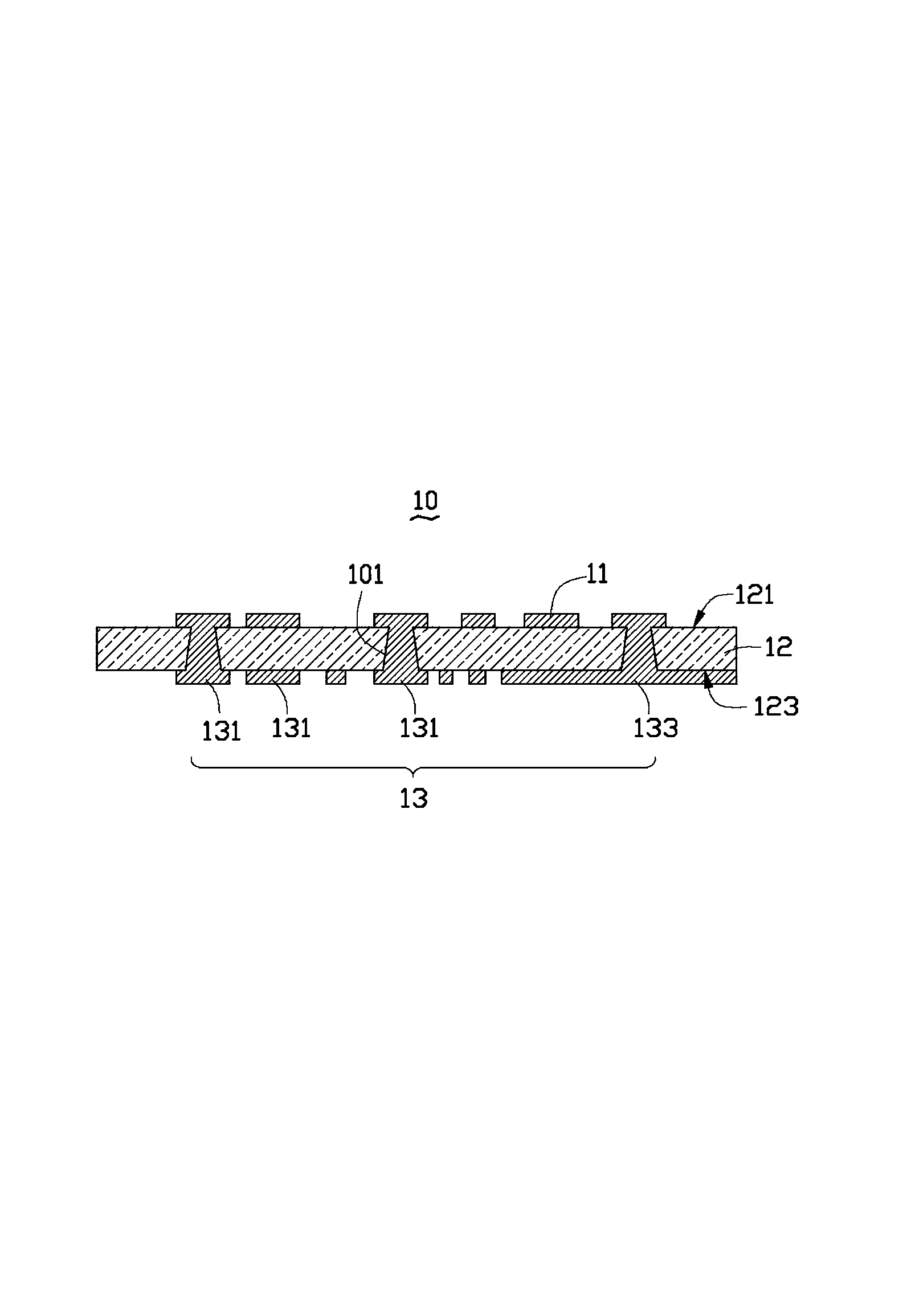
[0031] As a first step, see figure 1, providing a glass circuit substrate 10 . The glass circuit substrate 10 includes a first conductive circuit pattern 11 , a glass substrate 12 and a second conductive circuit pattern 13 stacked in sequence. The first conductive circuit pattern 11 is formed on the first surface 121 of the glass substrate 12 , and the second conductive circuit pattern 13 is formed on the second surface 123 . Both the first conductive circuit pattern 11 and the second conductive circuit pattern 13 are made of conductive materials such as copper, silver or aluminum b...


PUM


Abstract

The invention provides a manufacturing method of a multi-layer circuit board. The method includes providing a glass circuit substrate plate comprising a first conductive circuit pattern, a glass substrate, and a second conductive circuit pattern which is provided with a plurality of first bonding pads; pressing a first pressed substrate plate, comprising a first substrate layer and a first conductive material layer, on the glass circuit substrate plate, and allowing the first substrate layer to locate between the first conductive circuit pattern and a first conductive material layer; manufacturing the first conductive material layer into a third conductive circuit pattern, and electrically connecting the third conductive circuit pattern and the first conductive circuit pattern; forming a first bonding-proof layer, provided with a plurality of first openings corresponding to first bonding pad, on the surface of the glass circuit substrate plate to expose a plurality of the first bonding pads so as to form a multi-layer circuit board. The first conductive circuit pattern and the second conductive circuit pattern are connected electrically. The invention further provides a multi-layer circuit board manufactured by the method.

Description

technical field [0001] The invention relates to the manufacturing technology of circuit boards, in particular to a multilayer circuit board with long service life and a manufacturing method thereof. Background technique [0002] With the advancement of science and technology, printed circuit boards are widely used in electronic products. For the application of the circuit board, please refer to the literature Takahashi, A. Ooki, N. Nagai, A. Akahoshi, H. Mukoh, A. Wajima, M. Res. Lab, High density multilayer printed circuit board for HITAC M-880, IEEE Trans . on Components, Packaging, and Manufacturing Technology, 1992, 15(4): 418-425. [0003] A common printed circuit board has a base layer made of an organic resin material and conductive lines formed on the base layer. However, the thermal expansion coefficient of the organic resin material is quite different from that of the chip made of silicon chip mounted on the conductive circuit, which will easily cause the conduct...

Claims


Application Information

Patent Timeline
Patent Type & Authority Applications(China)
IPC IPC(8): H05K3/46H05K1/02
Inventor 许诗滨
Owner QI DING TECHNOLOGY QINHUANGDAO CO LTD
Why Eureka
Try Eureka