Integrated type both-way ultra-low capacitance TVS device and manufacturing method thereof

A manufacturing method and integrated technology, applied in semiconductor/solid-state device manufacturing, electrical solid-state devices, electrical components, etc., to improve device quality and avoid defects

Active Publication Date: 2013-12-25
HANGZHOU SILAN INTEGRATED CIRCUIT
View PDF4 Cites 4 Cited by
  • Summary
  • Abstract
  • Description
  • Claims
  • Application Information

AI Technical Summary

Problems solved by technology

[0023] The purpose of the present invention is to provide an integrated bidirectional ultra-low capacitance TVS device and its manufacturing method, to solve the problem that th

Method used


Image

  • Integrated type both-way ultra-low capacitance TVS device and manufacturing method thereof
  • Integrated type both-way ultra-low capacitance TVS device and manufacturing method thereof
  • Integrated type both-way ultra-low capacitance TVS device and manufacturing method thereof

Examples


Embodiment Construction

[0074] The integrated bidirectional ultra-low capacitance TVS device and its manufacturing method proposed by the present invention will be further described in detail below in conjunction with the accompanying drawings and specific embodiments. Advantages and features of the present invention will be apparent from the following description and claims. It should be noted that all the drawings are in a very simplified form and use imprecise scales, and are only used to facilitate and clearly assist the purpose of illustrating the embodiments of the present invention.

[0075] This embodiment provides a method for manufacturing an integrated bidirectional ultra-low capacitance TVS device, including:

[0076] S10: providing a first conductivity type substrate;

[0077] S11: forming a first conductivity type epitaxial layer on the first conductivity type substrate;

[0078] S12: forming a second conductivity type buried layer in the first conductivity type epitaxial layer;

[0...


PUM

PropertyMeasurementUnit
Resistivityaaaaaaaaaa
Thicknessaaaaaaaaaa

Abstract

The invention provides an integrated type both-way ultra-low capacitance TVS device and a manufacturing method thereof. The method comprises the step of providing a first electric conduction type substrate, the step of forming a first electric conduction type epitaxial layer on the first electric conduction type substrate, the step of forming a second electric conduction type epitaxial layer on the first electric conduction type epitaxial layer to form a diode D2, the step of forming an isolation structure and forming a first area, a second area and a third area, the step of forming first electric conduction type isolation connected with the first electric conduction type substrate in the first area, the step of forming a second electric conduction type trap in the third area, the step of forming a second electric conduction type injection area connected with the first electric conduction type isolation to form a diode Z1, the step of forming first electric conduction type injection areas in the second area and the second electric conduction type trap to form a diode D1 and a diode Z2, and the step of forming a first metal wire connecting the diode Z1 and the diode D1 and forming a second metal wire connecting the diode D1 and the diode Z2. Accordingly, the packaging defects are overcome, and the quality of the device is improved.

Description

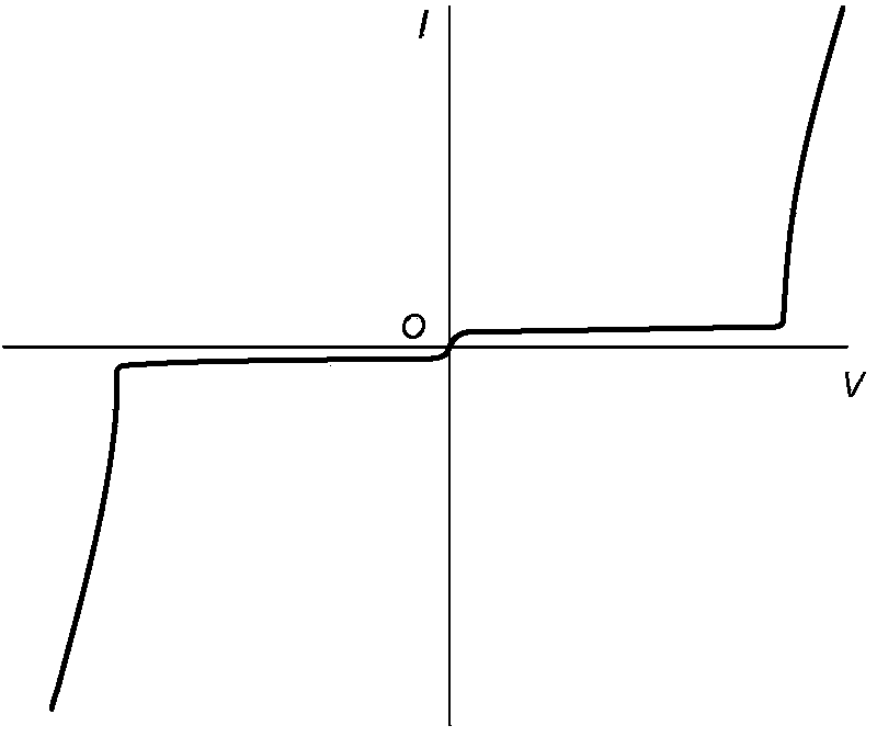
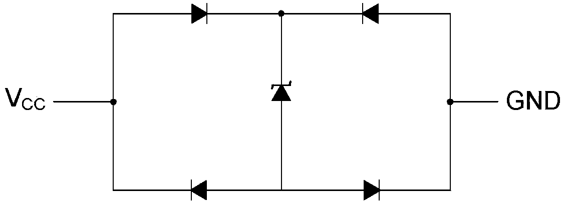
technical field [0001] The invention relates to the technical field of semiconductor manufacturing, in particular to an integrated bidirectional ultra-low capacitance TVS device and a manufacturing method thereof. Background technique [0002] Compared with unidirectional ultra-low capacitance TVS devices, bidirectional ultra-low capacitance TVS devices have conventional electrical I-V curves in both positive and negative directions (see figure 1 ) is basically symmetrical, so that in practical applications, it can protect both directions of the circuit at the same time, so the application range is wider. Usually, the capacitance of the power supply to ground in the bidirectional ultra-low capacitance TVS device can reach less than 0.3pF, and the ESD capability of both forward and reverse directions can reach greater than 8kV. There are roughly three types of bidirectional ultra-low capacitance TVS device structures currently on the market. [0003] The first type is to se...

Claims


Application Information

Patent Timeline
IPC IPC(8): H01L27/08H01L21/822H01L21/265
Inventor 张常军王平
Owner HANGZHOU SILAN INTEGRATED CIRCUIT
Why Eureka
Try Eureka