This helps you quickly interpret patents by identifying the three key elements:
Problems solved by technology
Method used
Benefits of technology
Problems solved by technology
However, the existing field effect transistors are limited by the drift diffusion mechanism, and the subthreshold slope cannot be lower than ln10 kTq, which makes it difficult to reduce the power supply voltage with the channel length under the same characteristics. The tunneling mechanism based on the PN junction The pass field effect transistor has attracted widespread attention due to its advantages of low power consumption and low subthreshold slope, and has become the main solution to break through this limitation.
Method used
Image
Click on the blue label to locate the original text in one second.
Reading with bidirectional positioning of images and text.
Examples
Embodiment 1
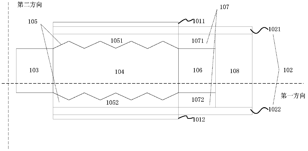
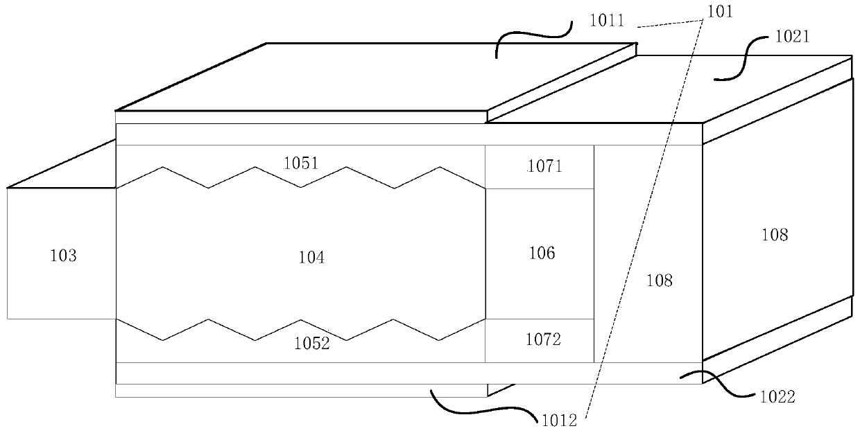
[0044] When the first source region, the second source region, the connection region and the drain region are cuboids, and the number of gate electrode layers is two layers, the formed tunneling field effect transistor is as follows: Figure 1~2 As shown, in this embodiment, the Figure 1~2 The shown double-gate tunneling field effect transistor is called a parallel structure double-gate field effect transistor. figure 1 is a cross-sectional view of a parallel-structure double-gate tunneling field-effect transistor along a first direction, figure 2 It is a perspective view of a double-gate tunneling field effect transistor with a parallel structure. The parallel structure double gate tunneling field effect transistor comprises a gate electrode layer 101, a gate dielectric layer 102, a first source region 103, an inner layer source region 104, an outer layer source region 105, a high resistance region 106, an extension region 107 and a drain region 108 .
[0045] The gate e...
Embodiment 2
[0066] Please refer to Figure 9-10 , in this example, the Figure 9-10 The shown double-gate tunneling field effect transistor is called a vertical structure double-gate tunneling field effect transistor. Figure 9 is a cross-sectional view of a vertical double-gate tunneling field effect transistor along a first direction, Figure 10 It is a perspective view of a vertical double-gate tunneling field effect transistor.
[0067] refer to figure 1 and Figure 9 It can be seen that the structure of the parallel structure and the vertical structure double-gate tunneling field effect transistor is basically the same, including the gate electrode layer 201, the gate dielectric layer 202, the first source region 203, the inner layer source region 204, the outer layer source region 205, the high The blocking region 206 , the extension region 207 , the drain region 208 , and the vertical double-gate tunneling field effect transistor further includes a substrate 209 , and the subst...
Embodiment 3
[0070] When the first source region, the second source region, the connection region and the drain region are cuboids, and the number of gate electrode layers is three layers, the formed tunneling field effect transistor is as follows: Figures 11 to 14 as shown, Figure 11 It is a perspective view of a tri-gate tunneling field effect transistor, Figure 12 is a cross-sectional view of the second source region of the tri-gate tunneling field effect transistor along the second direction, Figure 13 is a sectional view of the connection region of the tri-gate tunneling field effect transistor along the second direction, Figure 14 is a cross-sectional view of the tri-gate tunneling field effect transistor along the first direction.
[0071] Such as Figures 11 to 14 As shown, the tri-gate tunneling field effect transistor in this embodiment also includes an insulating layer 309 and a substrate layer 310; the insulating layer 309 covers the substrate layer 310 in the second di...
PUM
Abstract
The invention discloses a tunneling field effect transistor comprising a gate electrode layer, a gate dielectric layer, a source region, a connected region and a drain region. The source region comprises a first source region body and a second source region body, the second source region body comprises an inner layer source region main body and an outer layer source region main body, the connected region comprises an expansion region body and a high-resistance region body, the material doping type of the inner layer source region main body and the material doping type of the outer layer source region main body are opposite, the forbidden bandwidth of a material of the inner layer source region main body is smaller than that of a material of the outer layer source region main body, and the contact face formed due to the fact that the outer layer source region main body covers the inner layer source region main body is a curved face. The tunneling field effect transistor has the advantages that the contact face of the outer layer source region main body and the inner layer source region main body is of a curved face structure, the contact area of the outer layer source region main body and the inner layer source region main body is increased, the probability of tunneling of a carrier through the contact face is increased, and therefore on-state current is increased and a good current drive ability is achieved.
Description
technical field [0001] The present application relates to the field of semiconductor devices, in particular to a tunneling field effect transistor. Background technique [0002] With the development of integrated circuits, power consumption has gradually become an important performance indicator. Field-effect transistors are the basic unit of integrated circuits, and the development of field-effect transistors with excellent performance and low power consumption has become the goal of pursuit. After the introduction of double-gate and triple-gate structures, as well as high-k and stress silicon processes in the manufacture of field effect transistors, the performance of field effect transistors has been significantly improved. However, the existing field effect transistors are limited by the drift diffusion mechanism, and the subthreshold slope cannot be lower than ln10 kTq, which makes it difficult to reduce the power supply voltage with the channel length under the same c...
Claims
Application Information
Patent Timeline
Application Date:The date an application was filed.
Publication Date:The date a patent or application was officially published.
First Publication Date:The earliest publication date of a patent with the same application number.
Issue Date:Publication date of the patent grant document.
PCT Entry Date:The Entry date of PCT National Phase.
Estimated Expiry Date:The statutory expiry date of a patent right according to the Patent Law, and it is the longest term of protection that the patent right can achieve without the termination of the patent right due to other reasons(Term extension factor has been taken into account ).
Invalid Date:Actual expiry date is based on effective date or publication date of legal transaction data of invalid patent.

