Supercharge Your Innovation With Domain-Expert AI Agents!

Manufacturing method of light-emitting diode

A technology of light-emitting diodes and optical symmetry, which is applied to semiconductor devices, electrical components, circuits, etc., can solve problems affecting the light output rate of light-emitting diodes, and achieve the effect of improving the light output rate

Active Publication Date: 2016-04-13
TSINGHUA UNIV +1
View PDF5 Cites 0 Cited by
  • Summary
  • Abstract
  • Description
  • Claims
  • Application Information

AI Technical Summary

Problems solved by technology

[0004] However, in the light-emitting diodes prepared in the existing method, the near-field evanescent light waves (waves with an attenuation distance less than 20 nanometers) from the active layer cannot be emitted due to rapid attenuation during the outward radiation process, so they are limited to The interior of the semiconductor structure, until it is completely absorbed by the material in the light-emitting diode, affects the light extraction rate of the light-emitting diode

Method used


Image

  • Manufacturing method of light-emitting diode
  • Manufacturing method of light-emitting diode
  • Manufacturing method of light-emitting diode

Examples


Embodiment Construction

[0037] The light-emitting diode provided by the embodiment of the present invention and the manufacturing method thereof will be described in detail below with reference to the accompanying drawings.

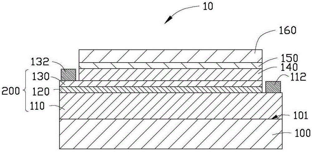
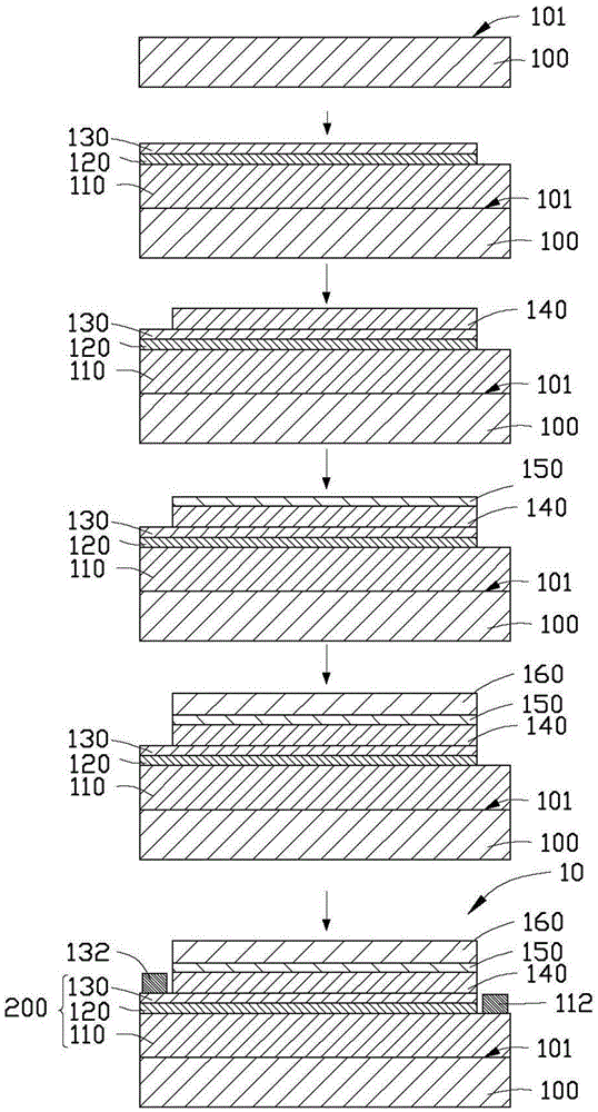
[0038] see figure 1 , the first embodiment of the present invention provides a light-emitting diode 10 with a lateral structure, which includes: it includes a substrate 100, a first semiconductor layer 110, an active layer 120, a second semiconductor layer 130, a first optically symmetrical layer 140 , a metal plasma generating layer 150 , a second optically symmetrical layer 160 , a first electrode 112 and a second electrode 132 . The first semiconductor layer 110, the active layer 120, the second semiconductor layer 130, the first optically symmetrical layer 140, the metal plasma generation layer 150, and the second optically symmetrical layer 160 are sequentially stacked on the surface of the substrate 100, And the first semiconductor layer 110 is disposed close to the subst...


PUM

PropertyMeasurementUnit
thicknessaaaaaaaaaa
thicknessaaaaaaaaaa
thicknessaaaaaaaaaa

Abstract

The invention relates to a method for preparing a light-emitting diode, which includes the following steps: providing a substrate, the substrate has an epitaxial growth surface; epitaxially growing a first semiconductor layer, an active layer and a second semiconductor layer on the epitaxial growth surface of the substrate in sequence. A semiconductor layer; a first optical symmetry layer is arranged on the surface of the second semiconductor layer away from the substrate; a metal plasma generation layer is arranged on the surface of the first optical symmetry layer away from the substrate; on the metal plasma generation layer forming a second optical symmetrical layer on the surface away from the base; forming a first electrode electrically connected to the first semiconductor layer; and forming a second electrode electrically connected to the second semiconductor layer.

Description

technical field [0001] The invention relates to a method for preparing a light-emitting diode, in particular to a method for preparing a light-emitting diode with a lateral structure. Background technique [0002] High-efficiency blue, green, and white light-emitting diodes made of gallium nitride semiconductor materials have remarkable features such as long life, energy saving, and environmental protection. They have been widely used in large-screen color displays, automotive lighting, traffic signals, multimedia displays, and optical communications. And other fields, especially in the field of lighting has broad development potential. [0003] A traditional light-emitting diode usually includes a substrate, an N-type semiconductor layer, a P-type semiconductor layer, an active layer arranged between the N-type semiconductor layer and the P-type semiconductor layer, and a P-type electrode (usually transparent electrode) and the N-type electrode disposed on the N-type semic...

Claims


Application Information

Patent Timeline
Patent Type & Authority Patents(China)
IPC IPC(8): H01L33/06H01L33/22
CPCH01L33/04H01L2933/0091H01L33/22H01L33/44H01L33/46
Inventor 朱钧张淏酥朱振东李群庆金国藩范守善
Owner TSINGHUA UNIV
Features
  • R&D
  • Intellectual Property
  • Life Sciences
  • Materials
  • Tech Scout
  • Unparalleled Data Quality
  • Higher Quality Content
  • 60% Fewer Hallucinations
Learn More