OLED device encapsulation structure

A packaging structure and device technology, applied in the direction of electric solid-state devices, semiconductor devices, organic semiconductor devices, etc., can solve problems affecting the service life of OLED devices 02

Active Publication Date: 2013-12-25
BOE TECH GRP CO LTD
View PDF5 Cites 53 Cited by
  • Summary
  • Abstract
  • Description
  • Claims
  • Application Information

AI Technical Summary

Problems solved by technology

[0005] However, the barrier of water vapor and oxygen in the film packaging structure has high requirements on the properties of the packaging film 03 itself, and water vapor and oxygen may pass through the gaps between the packaging films 03 of each layer and the gap between the packaging film 03 and the substrate 01. The gap between them enters the OLED device 02, or directly penetrates into the OLED device 02 through each layer of encapsulation film 03, thereby affecting the service life of the OLED device 02

Method used


Image

  • OLED device encapsulation structure
  • OLED device encapsulation structure
  • OLED device encapsulation structure

Examples


Embodiment Construction

[0026] The following will clearly and completely describe the technical solutions in the embodiments of the present invention with reference to the accompanying drawings in the embodiments of the present invention. Obviously, the described embodiments are only some, not all, embodiments of the present invention. Based on the embodiments of the present invention, all other embodiments obtained by persons of ordinary skill in the art without making creative efforts belong to the protection scope of the present invention.

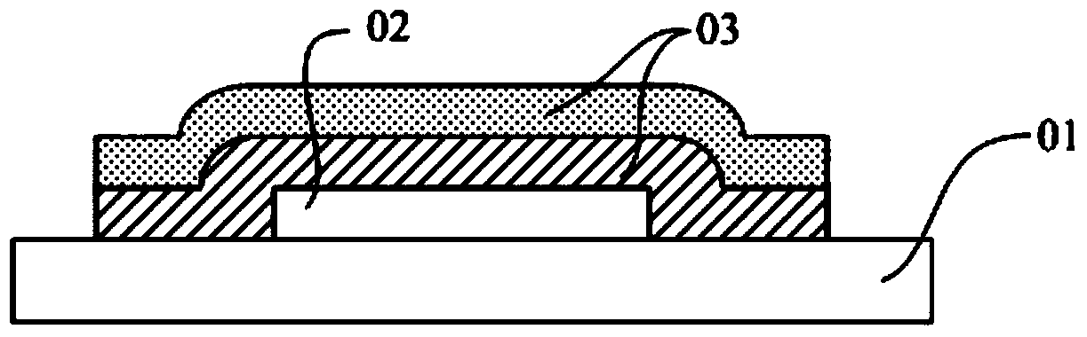
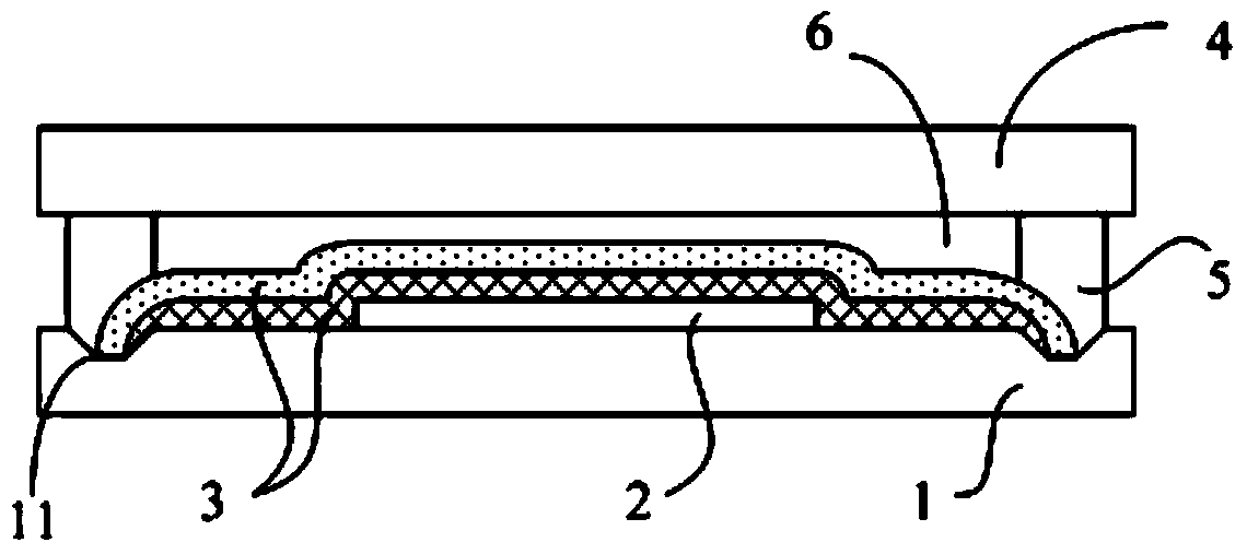
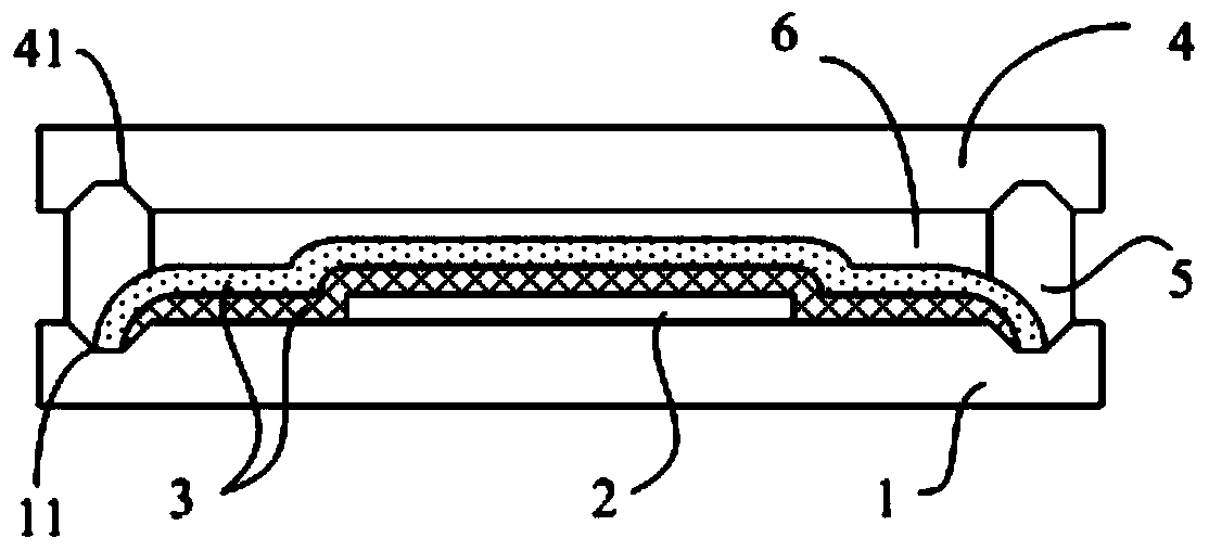
[0027] Please refer to figure 2 The encapsulation structure of the OLED device provided by the embodiment of the present invention includes an upper substrate 4 and a lower substrate 1 arranged oppositely, an OLED device 2 is arranged on the side of the lower substrate 1 facing the upper substrate 4, and an encapsulation film 3 is arranged on the OLED device 2; The edge of the lower substrate 1 and the edge of the upper substrate 4 are provided with a retaini...


PUM


Abstract

The invention relates to the encapsulation technical field, and discloses an OLED device encapsulation structure. The OLED device encapsulation structure comprises an upper substrate and a lower substrate, wherein the upper substrate and the lower substrate are arranged opposite to each other. An OLED device is arranged on the lower substrate, and an encapsulation thin film is arranged on the OLED device. The edge of the lower substrate is connected with the edge of the upper substrate in a sealed mode through a retaining wall. The edge of the side, facing the upper substrate, of the lower substrate is provided with a groove. The end, connected with the lower substrate, of the retaining wall is located in the groove of the lower substrate, and the periphery of the encapsulation thin film is sealed in the groove of the lower substrate through the retaining wall. The periphery of the encapsulation thin film is located in the groove formed in the edge of the lower substrate and is sealed in the groove through the retaining wall, a cavity between the upper substrate and the encapsulation thin film is filled with nitrogen or inert gas or resin or drying agents and the like to reduce water vapor and oxygen making contact with the encapsulation thin film, therefore, the influence of the water vapor and oxygen on the OLED device is lowered, and the service life of the OLED device is prolonged.

Description

technical field [0001] The invention relates to the technical field of encapsulation, in particular to an encapsulation structure of an OLED device. Background technique [0002] An OLED device refers to a device in which organic semiconductor materials and luminescent materials are driven by an electric field to cause light emission through carrier injection and recombination. OLED devices have many advantages and have bright prospects in the display field. OLED devices are very sensitive to water vapor and oxygen, and the water vapor and oxygen that penetrate into OLED devices are the main factors that affect the life of OLED devices; therefore, OLED devices are usually packaged with packaging structures to block oxygen and water vapor. [0003] Thin film encapsulation (TFE) is an encapsulation method for OLED devices, which has received extensive attention in the field of large-size OLED devices that pursue lightness and thinness and in the field of flexible OLED devices...

Claims


Application Information

Patent Timeline
Patent Type & Authority Applications(China)
IPC IPC(8): H01L33/52
CPCH01L2924/0002Y02E10/50H10K77/111H10K50/8426H10K2102/311H01L2924/00H01L31/0488H01L23/315H01L23/28
Inventor 张玉欣
Owner BOE TECH GRP CO LTD
Why Eureka
Try Eureka