
Electrode configurations for semiconductor devices

A semiconductor and device technology, applied in the field of semiconductor electronic devices, which can solve problems such as difficulty in manufacturing

Inactive Publication Date: 2014-01-08
TRANSPHORM INC
View PDF4 Cites 5 Cited by
  • Summary
  • Abstract
  • Description
  • Claims
  • Application Information

AI Technical Summary

Problems solved by technology

[0007] While sloped field plates are desirable for many applications, they can be difficult to reproducibly fabricate

Method used


Image

  • Electrode configurations for semiconductor devices
  • Electrode configurations for semiconductor devices
  • Electrode configurations for semiconductor devices

Examples


Embodiment Construction

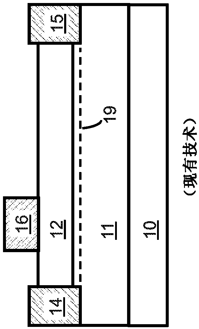
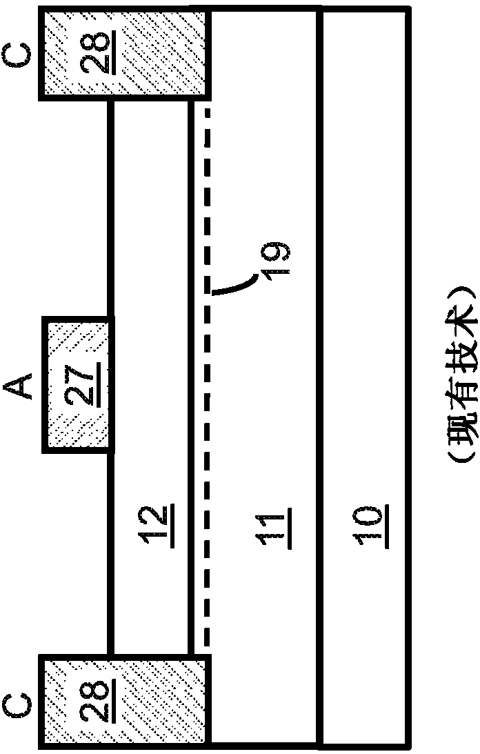
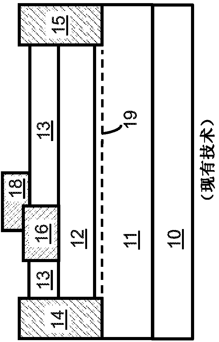
[0030] Devices based on III-N heterostructures are described. The electrodes of the device are designed such that the device can be fabricated reproducibly, can support high voltages with low leakage and, at the same time, can exhibit low resistance. Methods of forming the devices are also described. The III-N devices described herein may be, for example, transistors or diodes, and may be high voltage devices suitable for high voltage applications. In such a high voltage diode, when the diode is reverse biased, the diode is at least capable of supporting all voltages less than or equal to the high voltage in the application in which the diode is used, which may be, for example, 100V, 300V, 600V, 1200V, 1700V or higher. When a diode is forward biased, it is capable of conducting large currents with low turn-on voltage. The maximum allowable on-state voltage is the highest voltage that can be sustained in an application using a diode. When a high voltage transistor is biased...


PUM


Abstract

A III-N semiconductor device can include an electrode-defining layer having a thickness on a surface of a III-N material structure. The electrode-defining layer has a recess with a sidewall, the sidewall comprising a plurality of steps. A portion of the recess distal from the III-N material structure has a first width, and a portion of the recess proximal to the III-N material structure has a second width, the first width being larger than the second width. An electrode is in the recess, the electrode including an extending portion over the sidewall of the recess. A portion of the electrode-defining layer is between the extending portion and the III-N material structure. The sidewall forms an effective angle of about 40 degrees or less relative to the surface of the III-N material structure.

Description

technical field [0001] The present invention relates to semiconductor electronic devices and, in particular, to devices having electrodes connected to field plates. Background technique [0002] To date, modern power semiconductor diodes such as high voltage P-I-N diodes as well as power transistors such as power MOSFETs and insulated gate bipolar transistors (IGBTs) are usually fabricated from silicon (Si) semiconductor material. More specifically, silicon carbide (SiC) power devices have been investigated due to their excellent properties. III-nitride (III-N) semiconductor devices are now emerging, which are promising in carrying large currents and supporting high voltages while offering very low resistance, high-voltage device operation, and fast switching times. As used herein, the term III-N or III-nitride material, layer, device, etc. means x In y Ga z A material or device composed of N compound semiconductor materials, where x+y+z is about 1. [0003] exist figu...

Claims


Application Information

Patent Timeline
Patent Type & Authority Applications(China)
IPC IPC(8): H01L29/78H01L21/336H01L21/28
CPCH01L21/283H01L29/7787H01L29/6609H01L21/28581H01L29/6606H01L29/66462H01L29/778H01L21/76804H01L29/1608H01L29/417H01L29/42316H01L29/861H01L29/2003H01L29/66068H01L29/872H01L29/205
Inventor 尤瓦扎·多拉
Owner TRANSPHORM INC
Learn More