Capacitance type absolute pressure sensor and manufacturing method thereof
An absolute pressure sensor and a manufacturing method technology, applied in the field of sensors, can solve the problems that the airtightness of the bonding surface is not easy to be effectively guaranteed, the sensor cannot work normally for a long time, and the output drift of the micro-leakage sensor, etc., achieves reasonable structure and wide application range , the effect of high measurement accuracy
- Summary
- Abstract
- Description
- Claims
- Application Information
AI Technical Summary
Problems solved by technology
Method used
Image
Examples
Embodiment 1
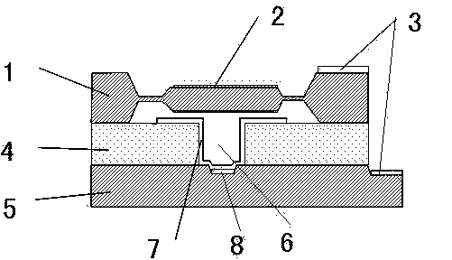
[0025] Such as figure 1 As shown, a glass-silicon composite pole plate is fixed under the silicon movable pole plate, and the silicon movable pole plate is fixed with a silicon oxide layer 2 on both sides of the silicon wafer layer 1 polished on both sides. One end side of layer 1 is fixed with a metal conductive layer 3, and the thickness of the silicon layer is 380-420 microns; the glass-silicon composite pole plate is that the glass layer 4 is fixed on the top of the single crystal silicon material layer 5, and the center of the glass layer is With a through hole 6, a metal layer 8 is fixed on the silicon chip corresponding to the through hole on the glass layer, and an electrode layer 7 is fixed above the metal layer; a metal layer is also fixed on one end of the single crystal silicon material layer. Conductive layer 3.
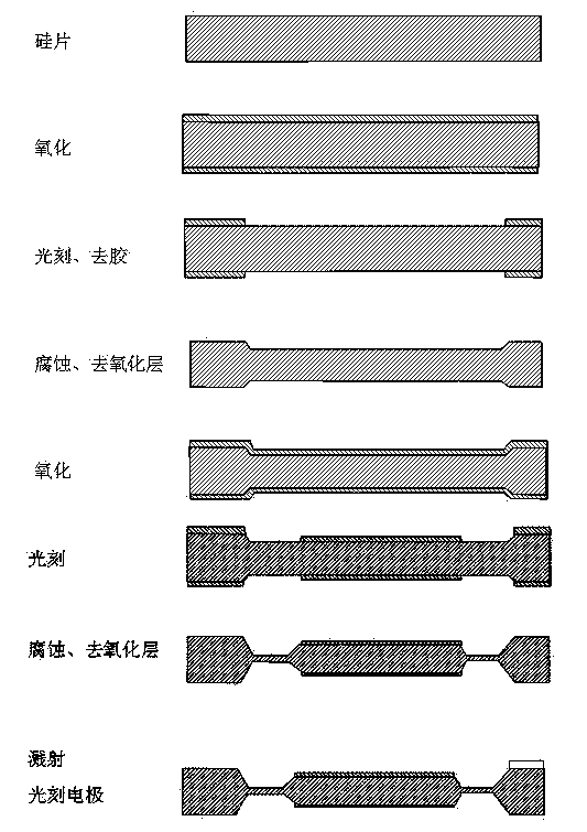
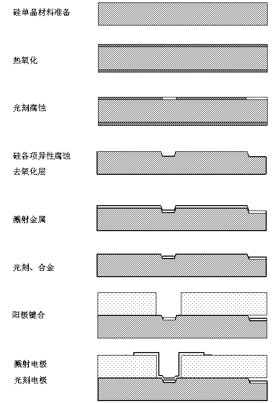
[0026] see Figure 2~4 , the manufacturing method of the above-mentioned capacitive absolute pressure sensor is as follows: wherein the manufacturing ...
Embodiment 2
[0035] Such as figure 1 As shown, a glass-silicon composite pole plate is fixed under the silicon movable pole plate. The silicon movable pole plate is fixed with a silicon oxide layer on the central island part of both sides of the silicon wafer layer polished on both sides, and one end of the silicon wafer layer is A metal layer is fixed on the side of the silicon wafer layer, and the thickness of the silicon wafer layer is 380-420 microns; the glass-silicon composite pole plate is a glass layer fixed above the monocrystalline silicon material layer, and a through hole is provided in the center of the glass layer. A metal layer is fixed at the position of the through hole of the chip relative to the glass layer and at one end, and an electrode layer is fixed above the metal layer at the position of the through hole of the silicon chip relative to the glass layer.
[0036] see Figure 2~4 , the manufacturing method of the above-mentioned capacitive absolute pressure sensor i...
PUM
| Property | Measurement | Unit |
|---|---|---|
| thickness | aaaaa | aaaaa |
| thickness | aaaaa | aaaaa |
| thickness | aaaaa | aaaaa |
Abstract
Description
Claims
Application Information


