
Semiconductor device manufacturing method

A device manufacturing method and semiconductor technology, applied in the fields of semiconductor/solid-state device manufacturing, semiconductor devices, electrical components, etc., can solve the problems of sub-threshold characteristic degradation, high defect density, self-heating effect, etc., to avoid self-heating problems, manufacturing methods The effect of simplicity and efficiency, reducing complexity

Active Publication Date: 2016-03-30
INST OF MICROELECTRONICS CHINESE ACAD OF SCI
View PDF5 Cites 0 Cited by
  • Summary
  • Abstract
  • Description
  • Claims
  • Application Information

AI Technical Summary

Problems solved by technology

However, SOI substrates have several problems: high wafer cost, high defect density, self-heating effect
For bulk silicon FinFET devices, the gate control ability of the bottom of the gate is weakened. When the impurities in the source and drain regions inevitably diffuse in the vertical direction, a sub-channel not controlled by the gate potential may be formed under the gate, that is, the phenomenon of source-drain punch-through, resulting in Turn-off current increases, subthreshold characteristics degrade

Method used


Image

  • Semiconductor device manufacturing method
  • Semiconductor device manufacturing method
  • Semiconductor device manufacturing method

Examples


Embodiment Construction

[0035] Hereinafter, the present invention is described by means of specific embodiments shown in the drawings. It should be understood, however, that these descriptions are exemplary only and are not intended to limit the scope of the present invention. Also, in the following description, descriptions of well-known structures and techniques are omitted to avoid unnecessarily obscuring the concept of the present invention.

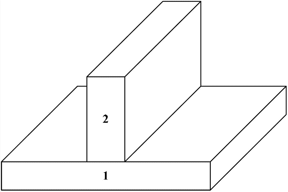
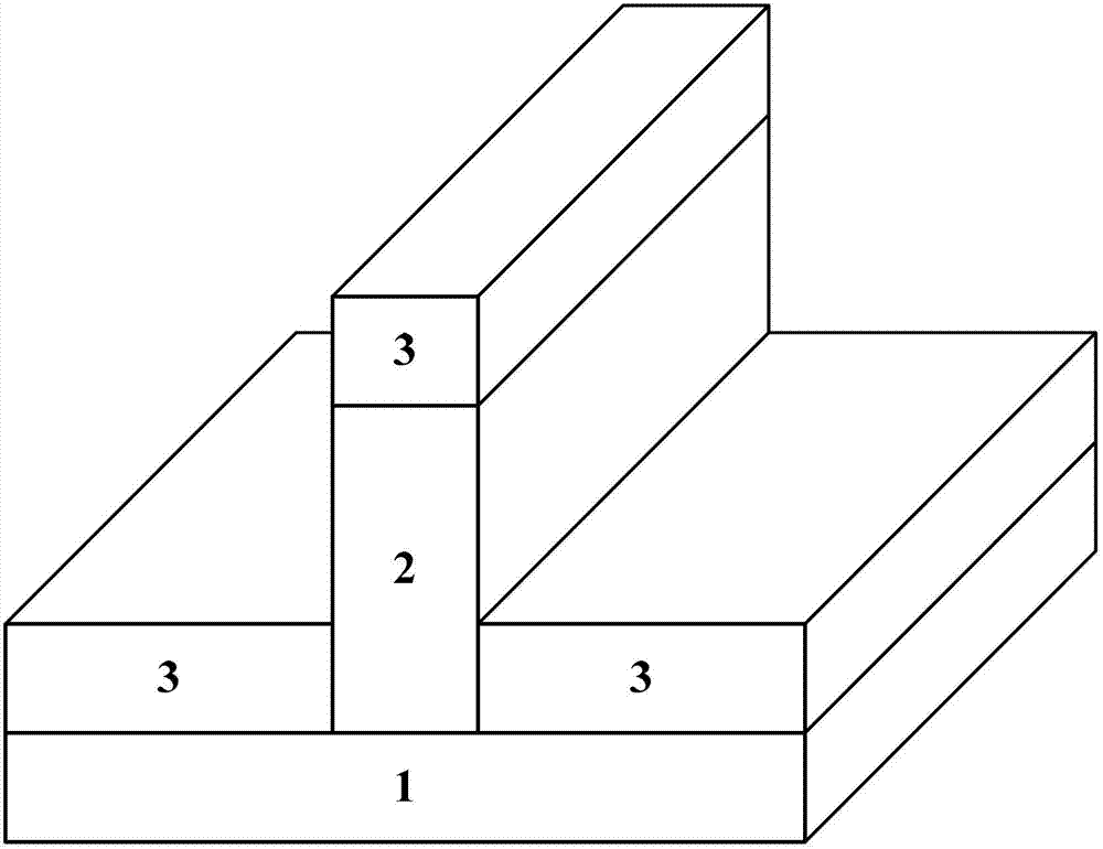
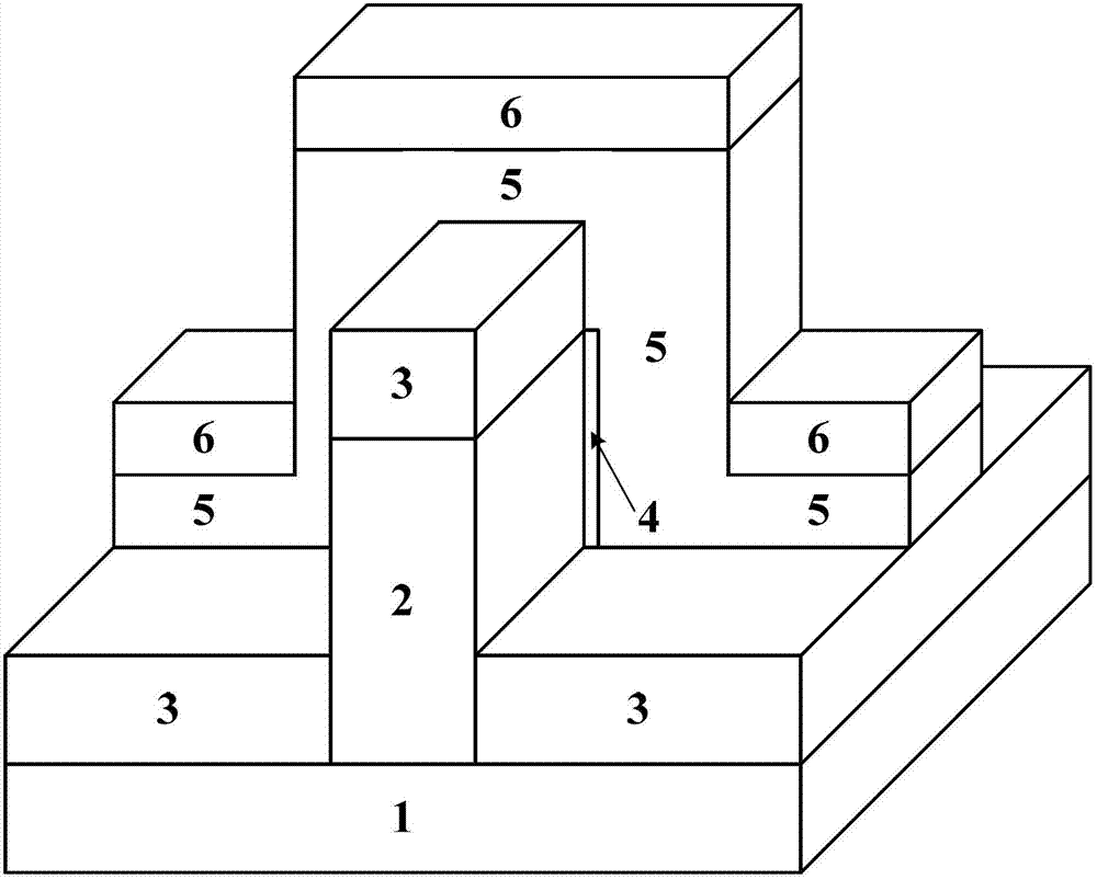
[0036] The present invention provides a FinFET manufacturing method, and its manufacturing process is shown in the attached Figure 1-9 .

[0037] First, see attached figure 1, Fin (fin-shaped semiconductor pillar) 2 is formed on the semiconductor substrate 1 . A semiconductor substrate 1 is provided, and a bulk silicon substrate is used in this embodiment. Fin2 is formed on a semiconductor substrate 1, and Fin2 has a side surface and a top surface. The method for forming Fin2 specifically includes: first coating a photoresist on the semiconductor subs...


PUM


Abstract

A semiconductor device manufacturing method is disclosed. A local isolation FinFET device structure is manufactured. A formed FinFET source drain area is located above a backfilling insulating material and is not directly connected with a semiconductor substrate. Only a channel region in a fin-shaped semiconductor column is connected with the semiconductor substrate so that a leakage current of the device is reduced; a source drain punch through problem is solved and a self-heating effect is avoided. In the manufacturing method, multiple layers of non-conformal hard mask layers are used so that a side wall of the device structure is exposed and a top surface is protected. Firstly, a grid graph and a position are defined and secondly, a source-drain local isolation technology (comprising partial etching and backfilling) is performed. Therefore, a self-registered technology of forming partial insulation on the substrate is realized; a complexity of a whole process is reduced; and the manufacturing method is simple and effective.

Description

technical field [0001] The present invention relates to the field of semiconductor device manufacturing methods, in particular, to a method for manufacturing FinFETs (fin field effect transistors) based on bulk silicon substrates. Background technique [0002] In the past 30 years, semiconductor devices have been proportionally reduced in accordance with Moore's law, the feature size of semiconductor integrated circuits has been continuously reduced, and the integration level has been continuously improved. As the technology node enters the deep sub-micron field, such as within 100nm or even within 45nm, the traditional field effect transistor (FET), that is, planar FET, begins to encounter the limitations of various basic physical laws, making its prospect of scaling down challenged . Many new structure FETs have been developed to meet the actual needs, among which FinFET is a new structure device with great potential for scaling down. [0003] FinFET, Fin Field Effect Tr...

Claims


Application Information

Patent Timeline
Patent Type & Authority Patents(China)
IPC IPC(8): H01L21/762H01L21/28H01L21/336
CPCH01L29/66795
Inventor 刘佳骆志炯
Owner INST OF MICROELECTRONICS CHINESE ACAD OF SCI
Learn More