
Method for adjusting turn-on voltage of fin type field effect transistor with polycrystalline silicon grid

A fin field effect, polysilicon gate technology, applied in circuits, electrical components, semiconductor devices, etc., can solve the problems of device channel mobility drop, source-drain punch-through, low turn-on voltage, etc., to improve process compatibility, The effect of high operating speed and reduced production cost

Pending Publication Date: 2021-10-26
GALAXYCORE SHANGHAI
View PDF0 Cites 0 Cited by
  • Summary
  • Abstract
  • Description
  • Claims
  • Application Information

AI Technical Summary

Problems solved by technology

[0008] The object of the present invention is to provide a method for adjusting the turn-on voltage of a fin field effect transistor with a polysilicon gate, which can effectively adjust the turn-on voltage of the fin field effect transistor, solve the source-drain punch-through problem caused by too low turn-on voltage, and avoid excessive High channel doping concentration reduces the channel mobility of the device, simplifies the process flow of transistor arrays with multiple turn-on voltages, improves process compatibility, and reduces manufacturing costs

Method used


Image

  • Method for adjusting turn-on voltage of fin type field effect transistor with polycrystalline silicon grid
  • Method for adjusting turn-on voltage of fin type field effect transistor with polycrystalline silicon grid
  • Method for adjusting turn-on voltage of fin type field effect transistor with polycrystalline silicon grid

Examples


Embodiment Construction

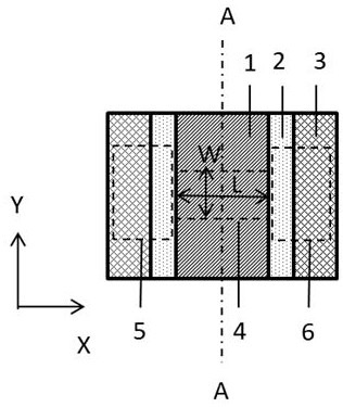
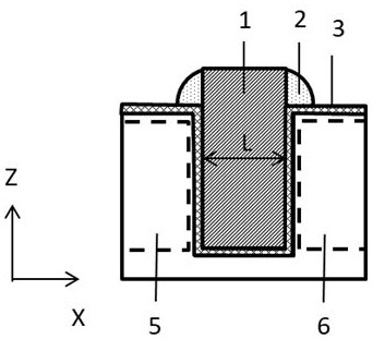
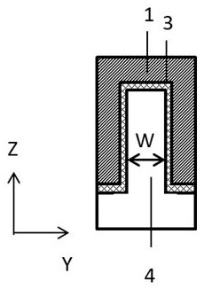
[0027] The invention provides a method for adjusting the turn-on voltage of a fin field effect transistor with a polysilicon gate. By changing the channel width of the semiconductor fin structure of the fin field effect transistor, the turn-on of the fin field effect transistor is adjusted and optimized Voltage, realizes the continuous adjustment of the transistor turn-on voltage, solves the problem of source-drain breakthrough caused by too low transistor turn-on voltage, and avoids the decrease of device channel mobility caused by too high channel doping concentration, so it can maintain a higher Running speed, no need to modify the preparation process steps, only need to change the channel width of the corresponding transistor on the design layout according to the needs, simplifies the process flow of transistor arrays with multiple turn-on voltages, improves process compatibility, and reduces preparation costs .

[0028] In the following detailed description of the preferr...


PUM

PropertyMeasurementUnit
widthaaaaaaaaaa

Abstract

According to the method for adjusting the turn-on voltage of the fin type field effect transistor with the polycrystalline silicon grid, the turn-on voltage of the fin type field effect transistor is adjusted and optimized by changing the channel width of the semiconductor fin structure of the fin type field effect transistor, and continuous adjustment of the turn-on voltage of the transistor is achieved. The problem of source-drain punch-through caused by too low threshold voltage of the transistor is solved, and reduction of device channel mobility caused by too high channel doping concentration is avoided, so that higher operation speed can be maintained, preparation process steps do not need to be modified, and only the channel width of the corresponding transistor needs to be changed on a design layout according to needs. The process flow of the transistor array with various starting voltages is simplified, the process compatibility is improved, and the preparation cost is reduced.

Description

technical field [0001] The invention relates to a method for adjusting the turn-on voltage of a fin field effect transistor with a polysilicon gate. Background technique [0002] Compared with traditional planar transistors, Fin Field Effect Transistors (FinFETs) can bring smaller footprints and better channel control capabilities due to their three-dimensional structure. Therefore, at the high-density complementary metal-oxide-semiconductor transistor (CMOS) process node, especially the process node below 28 nm, FinFET has become the main transistor structure used. [0003] According to functional requirements in the transistor array, it may be necessary to use transistors with different turn-on voltages. Traditional planar transistors change the device turn-on voltage by adjusting the channel doping concentration. However, since the channel structure of FinFET is thinner than that of traditional planar transistors, the doping process conventionally used to adjust the tur...

Claims


Application Information

Patent Timeline
Patent Type & Authority Applications(China)
IPC IPC(8): H01L29/78
CPCH01L29/785
Inventor 赵立新黄琨
Owner GALAXYCORE SHANGHAI
Learn More