AlGaN/GaN heterojunction vertical type field effect transistor with P type shielding layer and manufacturing method of field effect transistor

A field effect transistor, vertical field effect technology, applied in the field of power semiconductor devices, can solve the problems of oxide layer cracking or even breakdown, device life and reliability reduction, etc., to change current distribution, improve reliability, and improve breakdown voltage. Effect

Active Publication Date: 2019-06-14
XIDIAN UNIV
View PDF5 Cites 0 Cited by
  • Summary
  • Abstract
  • Description
  • Claims
  • Application Information

AI Technical Summary

Problems solved by technology

In addition, when the device is turned off, due to the high voltage, a high electric field will be generated in the gate dielectric layer, which will easily cause the oxide layer to break or even break down, and the life and reliability of the device will also be greatly reduced.

Method used


Image

  • AlGaN/GaN heterojunction vertical type field effect transistor with P type shielding layer and manufacturing method of field effect transistor

Examples


Embodiment Construction

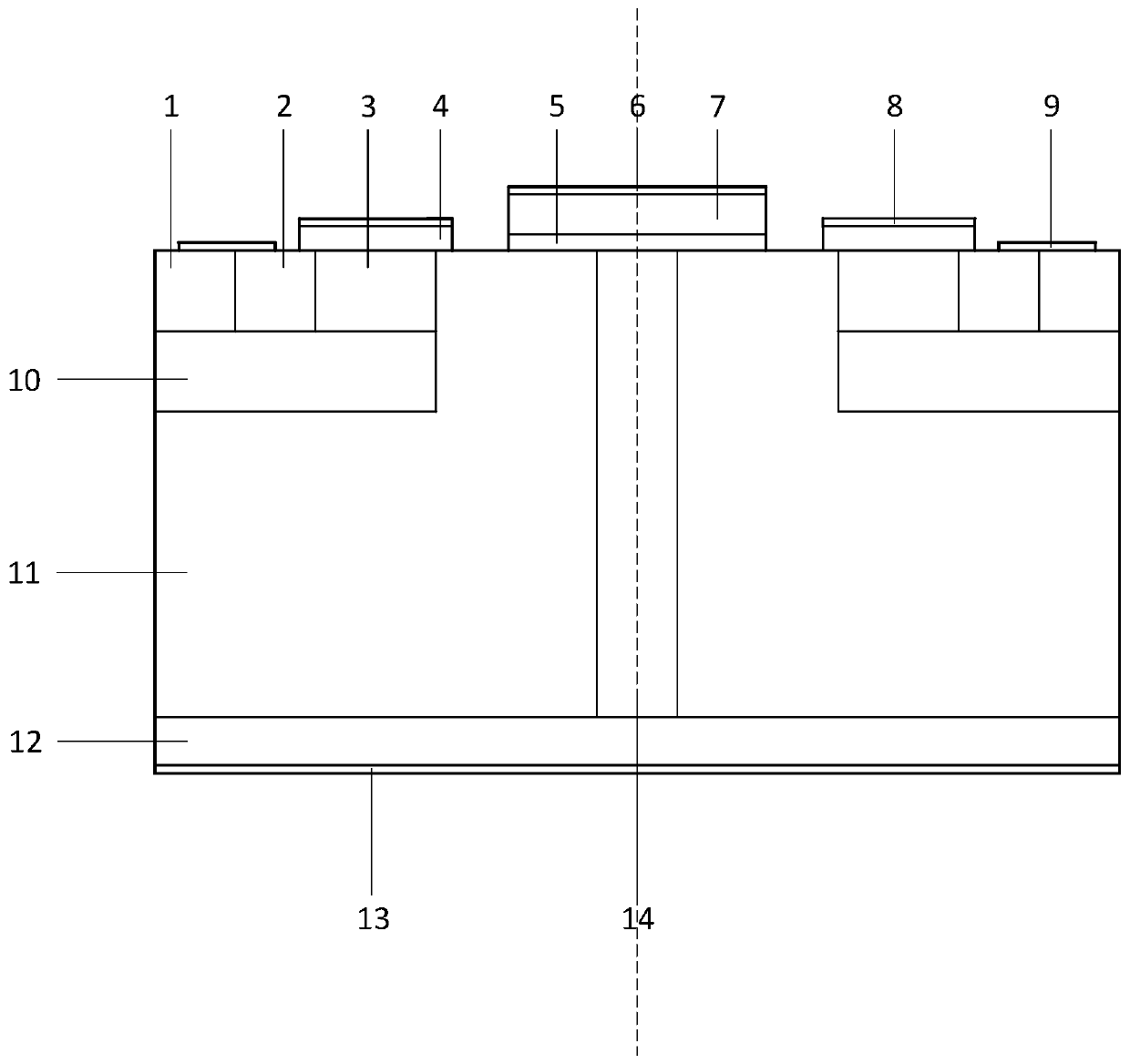
[0047] The present invention will be described below by taking an N-channel AlGaN / GaN heterojunction vertical field effect transistor with a P-type shielding layer as an example in conjunction with the accompanying drawings.

[0048] like figure 1 As shown, in the structure of this embodiment, the drift region is divided into two parts: the lightly doped drift region 11 epitaxially grown on the substrate and the heavily doped drift region 14 formed by ion implantation in the middle of the lightly doped drift region. Corresponding to the middle part of the device, an ALGaN layer 5 is heteroepitaxially grown on the surface of the heavily doped drift region 14 and the adjacent lightly doped drift region 10 on both sides; the surface of the ALGaN layer is provided with an active dielectric layer 7 covering the interface of the 2DEG ; The three sources are connected together. Using the AlGaN / GaN heterojunction as part of the conductive channel improves the contradictory relationsh...


PUM


Abstract

The invention provides an AlGaN / GaN heterojunction vertical type field effect transistor with a P type shielding layer and a manufacturing method of the field effect transistor. The device is mainly characterized in that the P type shielding layer is adopted, and meanwhile, a current low-resistance conducting channel is formed by virtue of the two-dimensional electron gas and a special drift region of the AlGaN / GaN heterojunction. Due to the effect of the P type shielding layer, the concentration of the channel can be reduced to obtain a proper threshold voltage. When the device is switched off, the P type shielding layer effectively reduces the peak electric field in a gate dielectric layer, and the reliability of the device is improved; the two-dimensional electron gas introduces new charges, so that the electric field distribution in the device is changed, the breakdown voltage is improved, and meanwhile, the contradiction between the breakdown voltage and the drift region concentration is weakened. When the device is conducted, the current distribution of the traditional vertical type field effect transistor is changed due to the new conductive channel, so that the relatively low on resistance can be realized under the condition that the concentration of the drift region is relatively low.

Description

technical field [0001] The invention relates to the field of power semiconductor devices, in particular to an AlGaN / GaN heterojunction vertical field effect transistor with a P-type shielding layer. Background technique [0002] As one of the cores of the third-generation semiconductor materials, gallium nitride is special in that it has a polarization effect compared with Si and silicon carbide (SiC). The AlGaN / GaN heterojunction forms a high-density two-dimensional electron gas (two dimensional electron gas, 2DEG) at the heterojunction interface through spontaneous polarization and piezoelectric polarization effects. The high mobility in the channel leads to the low on-resistance of AlGaN / GaN HEMTs. However, the Schottky gate AlGaN / GaN HEMT device has a large reverse leakage, which leads to the deterioration of key performances such as breakdown voltage, efficiency, and gain of the device. [0003] In wide bandgap semiconductors, the impurity diffusion rate is very low, ...

Claims


Application Information

Patent Timeline
Patent Type & Authority Applications(China)
IPC IPC(8): H01L29/778H01L29/06H01L21/335
Inventor 段宝兴王彦东杨珞云杨银堂
Owner XIDIAN UNIV
Why Eureka
Try Eureka