Gallium nitride lateral transistor with AlGaN/GaN heterojunction and manufacturing method of gallium nitride lateral transistor

A lateral transistor and heterojunction technology, which is applied in the manufacture of semiconductor/solid-state devices, semiconductor devices, electrical components, etc., can solve the difficulties of AlGaN/GaN heterojunction transistors, etc., and achieve the effect of improving performance and reducing peak electric field.

Active Publication Date: 2019-05-28
XIDIAN UNIV
View PDF4 Cites 1 Cited by
  • Summary
  • Abstract
  • Description
  • Claims
  • Application Information

AI Technical Summary

Problems solved by technology

However, because AlGaN / GaN heterojunction transistors have a special withstand voltage mechanism, it is very difficult to obtain high withstand voltage AlGaN / GaN heterojunction transistors

Method used


Image

  • Gallium nitride lateral transistor with AlGaN/GaN heterojunction and manufacturing method of gallium nitride lateral transistor

Examples


Embodiment Construction

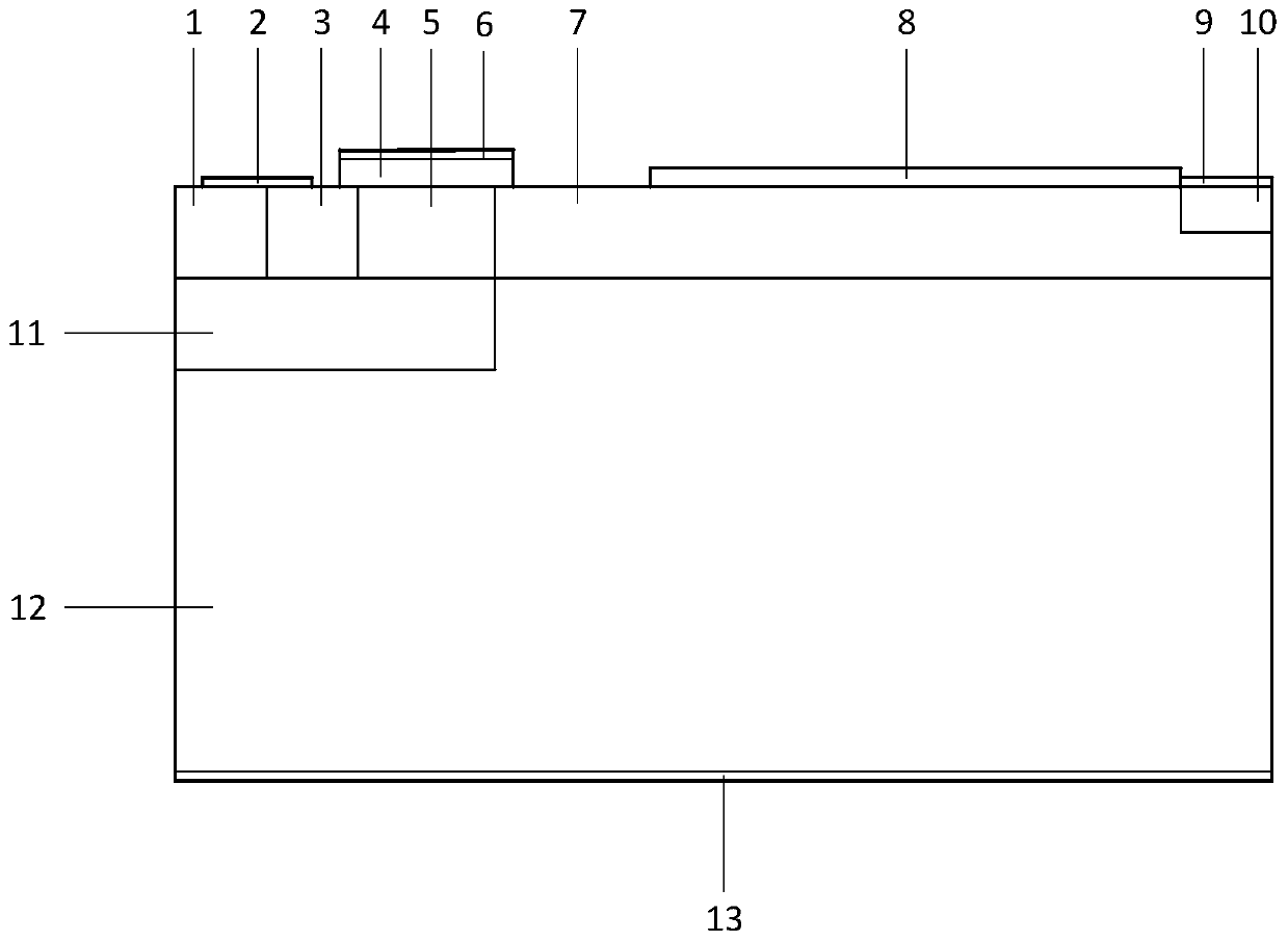
[0036] The present invention will be described below by taking a novel gallium nitride lateral transistor with an N-channel AlGaN / GaN heterojunction as an example in conjunction with the accompanying drawings.

[0037] Such as figure 1 As shown, the structure of this embodiment includes:

[0038] Substrates of semiconductor materials;

[0039] a drift region located on the surface of the substrate;

[0040] A base region, a source region, and a channel substrate contact formed by ion implantation based on one end of the drift region; the surface of the base region is covered with a gate dielectric layer;

[0041] A drain region formed by ion implantation based on the other end of the drift region;

[0042] Wherein, the substrate is a P-type GaN material, and the drift region is an N-type GaN material; a P-type shielding layer is also formed by ion implantation at the base region, the source region, and the substrate below the channel substrate contact;

[0043] The surface...


PUM


Abstract

The invention provides a gallium nitride lateral transistor with an AlGaN / GaN heterojunction and a manufacturing method of the gallium nitride lateral transistor. A partial drift region of the transistor is an AlGaN / GaN heterojunction; the AlGaN / GaN heterojunction forms high-density two-dimensional electron gas (2DEG) at the interface of the heterojunction through spontaneous polarization and piezoelectric polarization effects; and the two-dimensional electron gas has very high mobility, so that the novel gallium nitride lateral transistor with the AlGaN / GaN heterojunction has very low on-resistance. When the transistor is turned off, the 2DEG is exhausted; and meanwhile, a new electric field peak is introduced to the surface of the transistor, so that the peak electric field at the edge of the gate of the lateral transistor is reduced, and the breakdown voltage of the transistor is improved.

Description

technical field [0001] The invention relates to the field of power semiconductor devices, in particular to a lateral semiconductor field effect transistor. Background technique [0002] Lateral semiconductor field effect transistors have the advantages of easy integration, good thermal stability, good frequency stability, low power consumption, multi-subconduction, small power drive, and high switching speed. They are the core of intelligent power circuits and high-voltage devices. Due to the growing market demand for portable power management and automotive electronics, it is receiving increasing attention across the globe. [0003] The specific on-resistance of the high-voltage lateral double-diffused transistor increases with the 2.0th power of the breakdown voltage, which greatly limits its application in the high-voltage field. A technology of reducing the device surface electric field (Reduced Surface Field, RESURF) was proposed in 1979, which can well alleviate the c...

Claims


Application Information

Patent Timeline
Patent Type & Authority Applications(China)
IPC IPC(8): H01L29/778H01L21/335
Inventor 段宝兴王彦东黄芸佳杨银堂
Owner XIDIAN UNIV
Why Eureka
Try Eureka