

Photosensor chip package structure
A technology of chip packaging structure and optical sensing chip, which is applied in the direction of semiconductor/solid-state device parts, semiconductor devices, electrical components, etc., can solve the problems that the packaging area cannot be reduced, the packaging structure is complicated, etc., and the complex packaging structure and manufacturing process can be simplified. , reduce optical signal interference, and reduce the package area
- Summary
- Abstract
- Description
- Claims
- Application Information
AI Technical Summary
Problems solved by technology
Method used
Image

Examples
Embodiment Construction
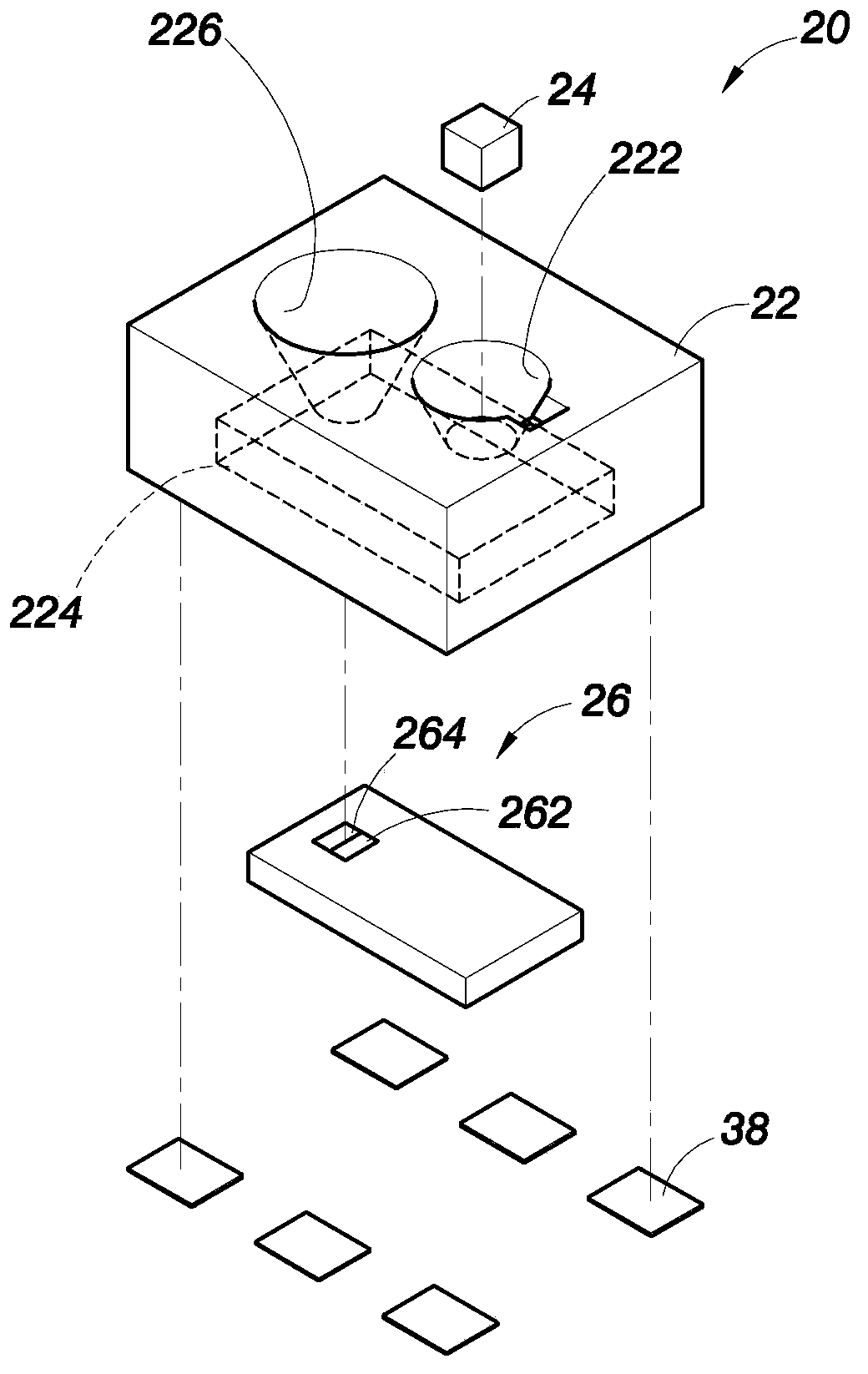
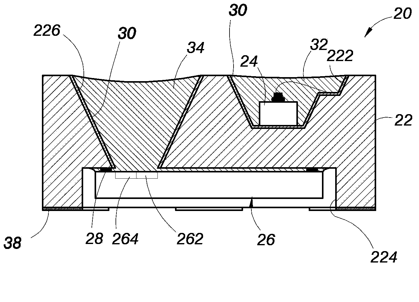
[0021] Please refer to FIG. 2(a), FIG. 2(b), FIG. 2(c) and FIG. 2(d) together, which are respectively a perspective view, a cross-sectional view, a top view, and a bottom view of the light-sensing chip package structure of the present invention. As shown in the figure, the light-sensing chip package structure 20 of the present invention mainly includes a substrate 22; a light-emitting chip 24; and an optical sensor chip 26.
[0022] The substrate 22 includes a first groove 222, a second groove 224 and a light guiding groove 226. The substrate 22 has opacity. The opening end directions of the first groove 222 and the second groove 224 are different, and the first groove 222 and the second groove 224 are at least partially overlapped. One open end of the light guiding groove 226 is on the same side as the open end of the first groove 222, and the other open end is connected to the second groove 224.
[0023] The light emitting chip 24 is disposed in the first groove 222, and the li...
PUM
 Abstract
Description
Claims
Application Information