Integrated circuit chip programmable and operation method

A technology of integrated circuits and circuit chips, applied in the field of integrated circuit chips with programmable functions and characteristics, can solve the problems of increasing cost and complexity of the manufacturing process, and achieve the effect of compensating for the possibility of failure

Active Publication Date: 2006-05-24
AVAGO TECH INT SALES PTE LTD
View PDF5 Cites 7 Cited by
  • Summary
  • Abstract
  • Description
  • Claims
  • Application Information

AI Technical Summary

Problems solved by technology

However, implementing E2PROM requires performing additional processing steps to fabricate sili

Method used


Image

  • Integrated circuit chip programmable and operation method
  • Integrated circuit chip programmable and operation method
  • Integrated circuit chip programmable and operation method

Examples


Example Embodiment

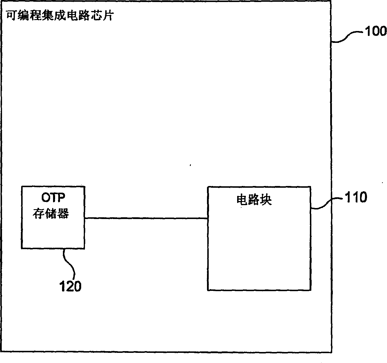
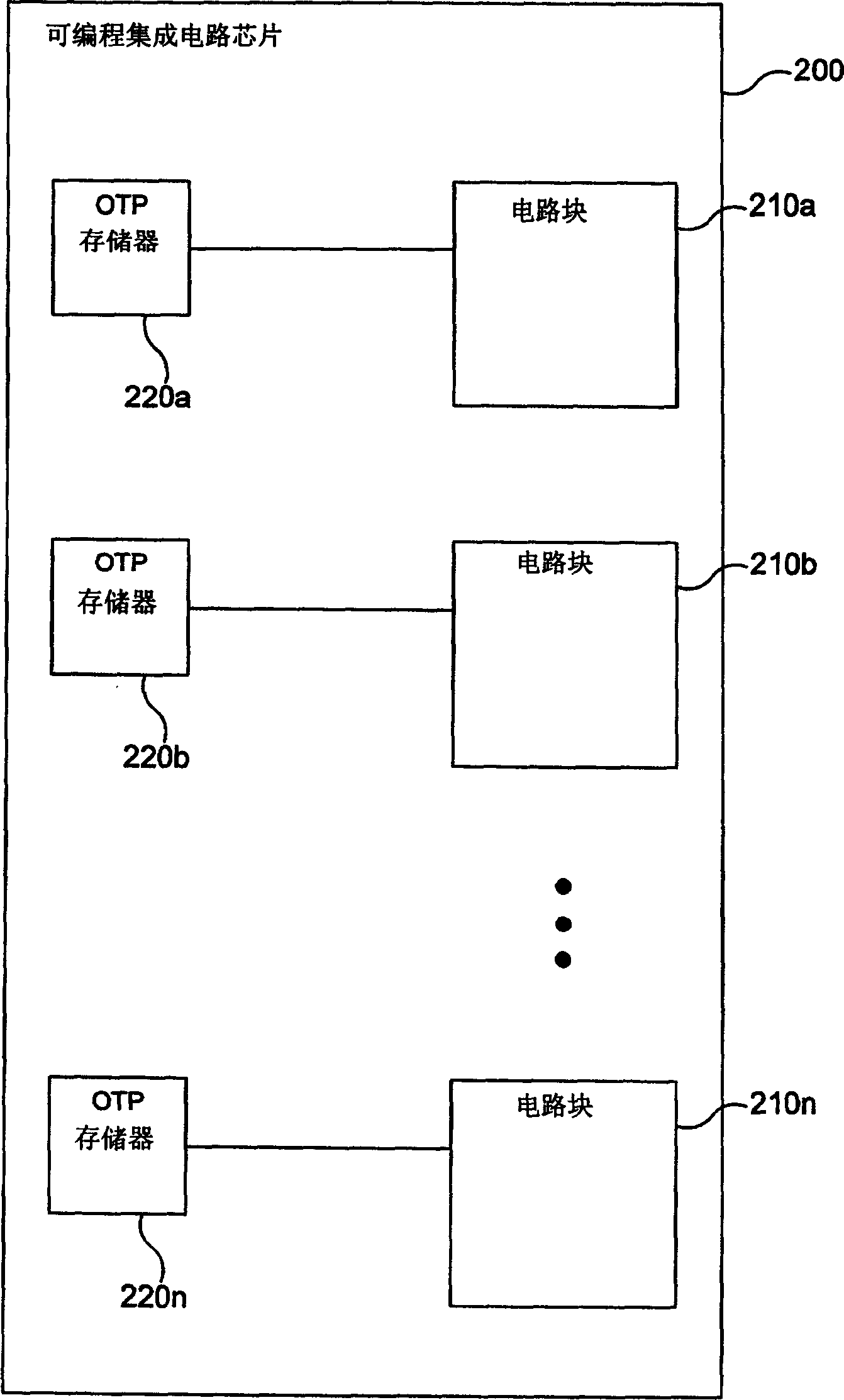
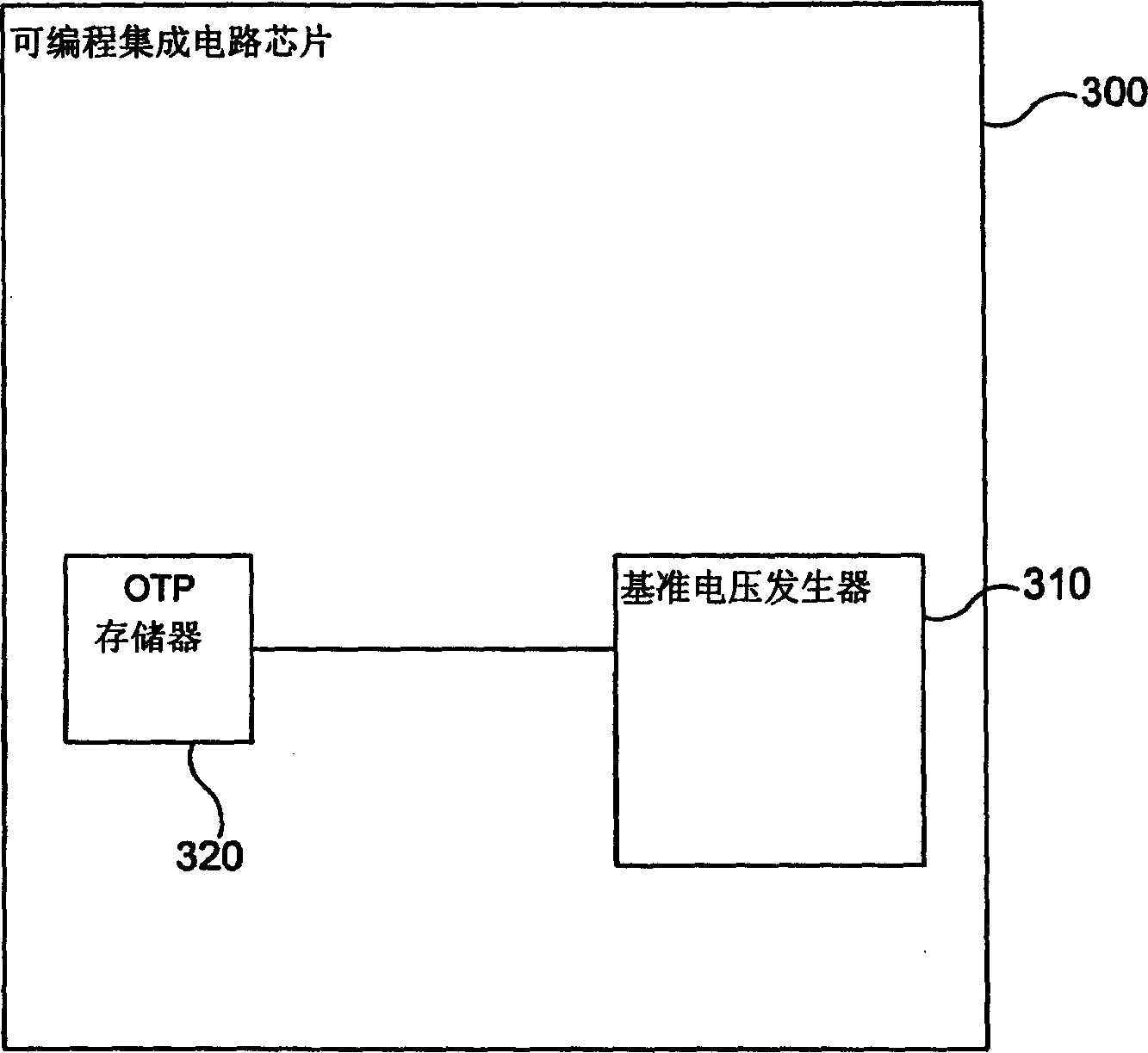
[0060] figure 1 A programmable integrated circuit chip 100 with programmable circuit blocks is shown in accordance with one embodiment of the present invention. like figure 1 As shown, the programmable integrated circuit chip 100 includes a circuit block 110 connected to an OTP memory 120 .

[0061] Circuit block 110 includes logic for performing one or more functions of programmable integrated circuit chip 100 . For example, this function may include providing a reference voltage or performing a power supply sequencing function. However, these examples do not limit the present invention, and those of ordinary skill in the art can easily understand that the circuit block 100 can also perform many other functions.

[0062] OTP memory 102 includes one or more OTP storage units. These OTP memory cells may be arranged as an array or as a group of one or more cells. Each OTP memory cell includes a nonvolatile storage element and a fuse element. The storage element can store l...


PUM


Abstract

The invention discloses an integrated circuit chip with programmable functions and features and its operating method, wherein a one-time programmable (OTP) memory is used to realize the function of a non-volatile memory. The OTP memory may be based on multi-state fuses and gate oxide fuses. Because the OTP memory is very small, it occupies a smaller package area than metal fuses. In addition, since OTP memory can be implemented as part of a standard CMOS process, this approach is less costly and less complex than using electrically erasable programmable read-only memory (E2PROM).

Description

technical field [0001] The present invention relates to integrated circuit chips, and more particularly, the present invention relates to integrated circuit chips having programmable functions and features. Background technique [0002] During and / or after the manufacture of an integrated circuit chip, it is often desirable to be able to change its function and characteristics. To do this, the chip can be designed in such a way that these characteristics are programmed using on-chip memory. Typically, the on-chip memory required for this programmability is implemented by, for example, metal fuses and / or electrically erasable programmable read-only memory (E2PROM). [0003] For example, metal fuses have been used to tune precise voltage references in silicon. Metal fuses typically occupy a relatively large area in silicon, limiting the number of fuses that can be included on a single chip. Because of this limitation, the programmability achieved using this approach is rath...

Claims


Application Information

Patent Timeline
IPC IPC(8): H01L27/00H01L23/525
Inventor 尼尔·Y·金皮特·沃恩坎普
Owner AVAGO TECH INT SALES PTE LTD
Why Eureka
Try Eureka