Semiconductor device and manufacturing method thereof

a semiconductor device and manufacturing method technology, applied in the direction of semiconductor devices, semiconductor/solid-state device details, electrical apparatus, etc., can solve the problems of large packaging area, difficult to remove semiconductor devices, complicated manufacturing steps, etc., and achieve the effect of reducing the packaging area

Inactive Publication Date: 2005-01-04
SEMICON COMPONENTS IND LLC
View PDF13 Cites 8 Cited by
  • Summary
  • Abstract
  • Description
  • Claims
  • Application Information

AI Technical Summary

Benefits of technology

Preferably, the semiconductor device of the present invention, the glass plate is employed to seal the semiconductor element in the hollow airtight portion. Therefore, the adhered state can be checked by the visual inspection, and also the removal of the semiconductor device in which the adhesion failure is caused can be facilitated.
Preferably, the semiconductor device of the present invention, the via holes are provided in the substrate. Then, internal elements can be connected electrically to the external connecting terminals, whereby no lead extended from the substrate to the outside is needed. Therefore, the packaging area can be reduced extremely when the semiconductor devices are packaged onto the printed board.

Problems solved by technology

However, in the semiconductor device in the conventional art, there is the subject that, since the base substrate 1 and the cap 3 are mounted on the lead frame every element, the manufacturing steps become complicated and are not suited for the mass production.
Also, there is the problem that, since the semiconductor chip 5 is sealed in the airtight space 7 that is constructed by the cap 3 made of ceramic, etc., the adhesion state cannot be checked by the visual inspection and thus it is difficult to remove the semiconductor device in which the adhesion failure is caused.
In addition, there is the problem that, since the above semiconductor device has the structure to project the lead 2 from the base substrate 1, a packaging area is large when such semiconductor device is packaged onto the printed circuit board.
But, in the conventional art, there is no overcurrent protection element that meets the light weight and the small size.
Thus, there is the drawback that the increase in size of the electronic device is brought about.

Method used


Image

  • Semiconductor device and manufacturing method thereof
  • Semiconductor device and manufacturing method thereof
  • Semiconductor device and manufacturing method thereof

Examples


Embodiment Construction

Embodiments of the present invention will be explained in detail with reference to the drawings hereinafter.

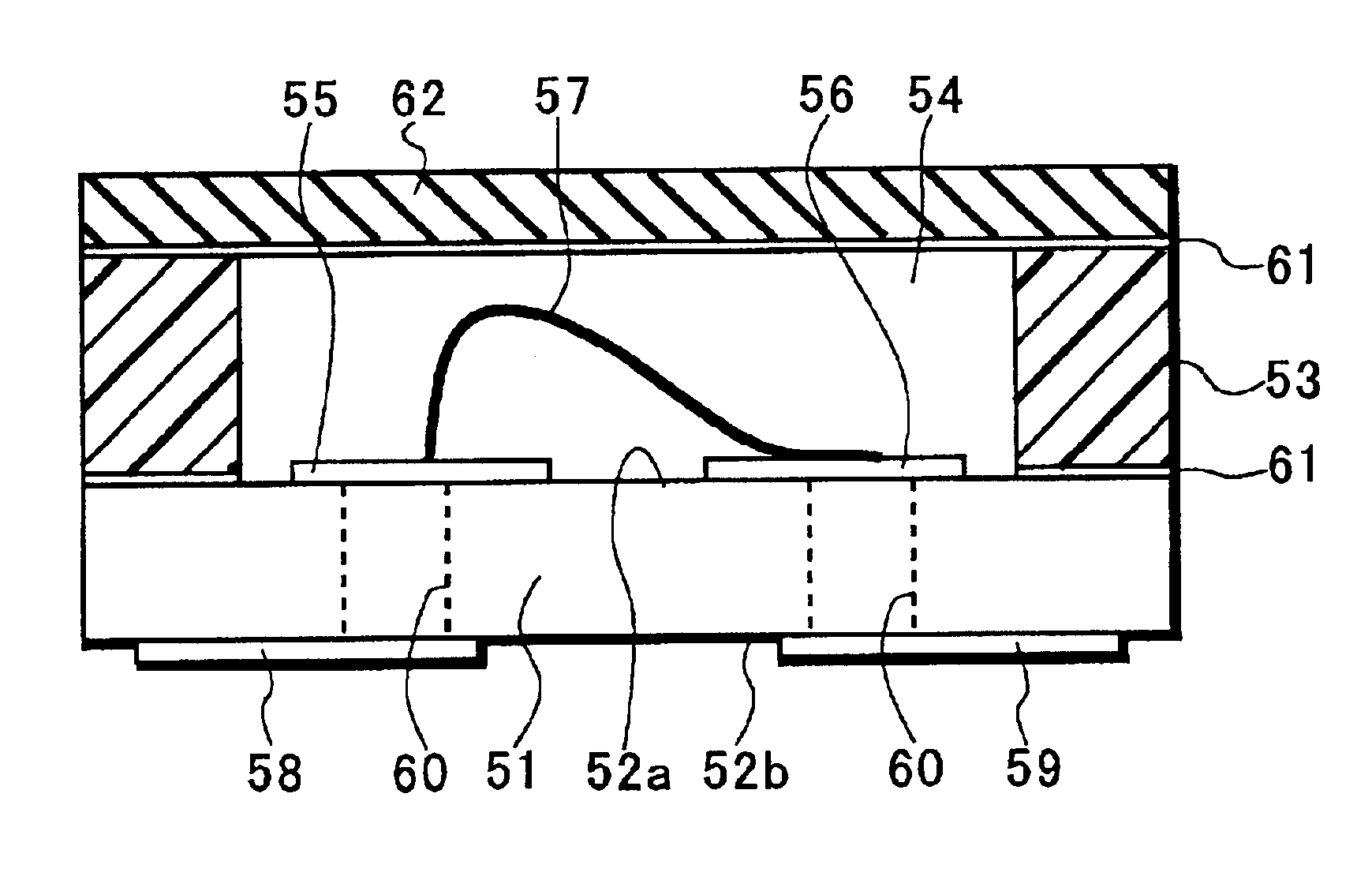
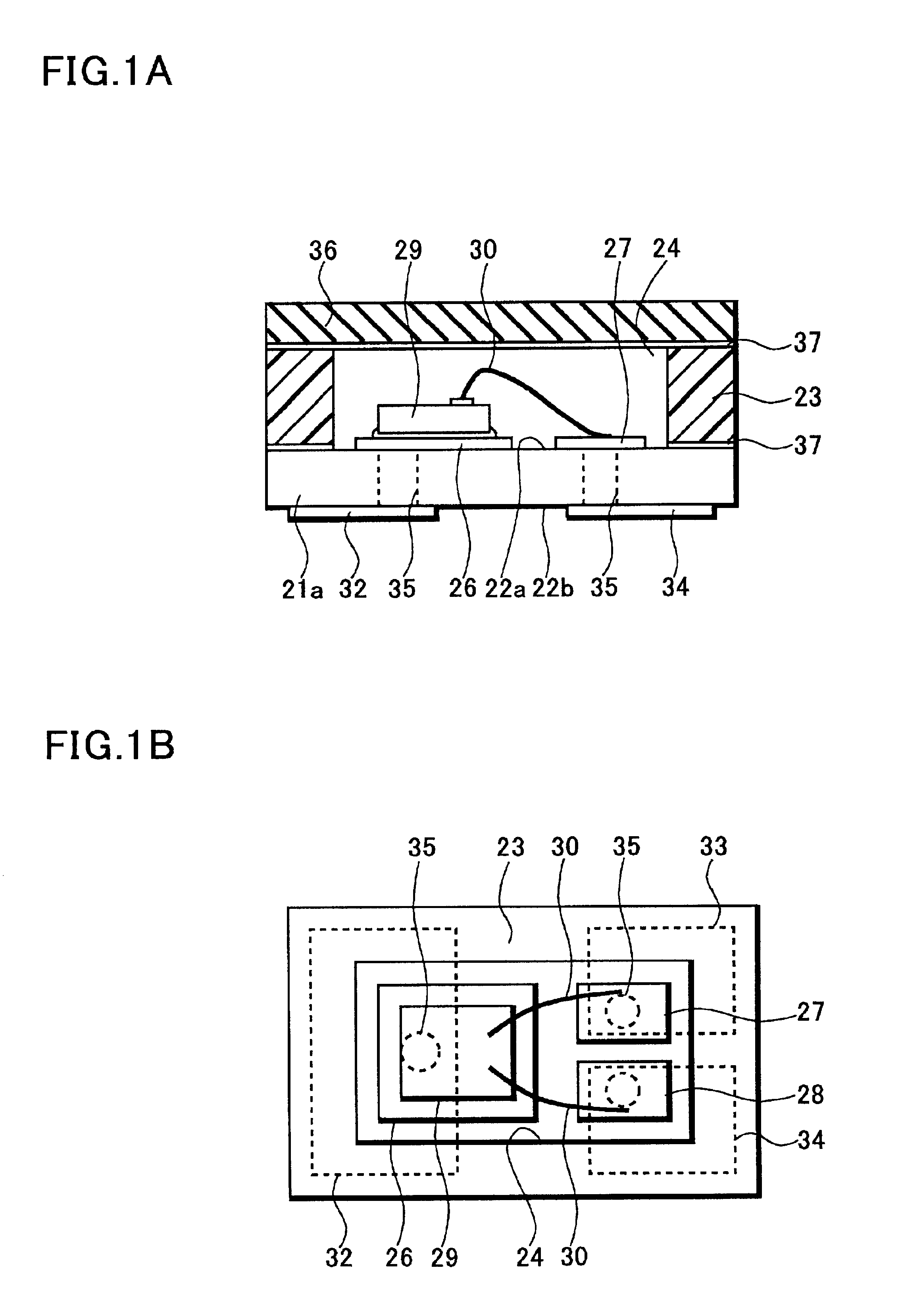
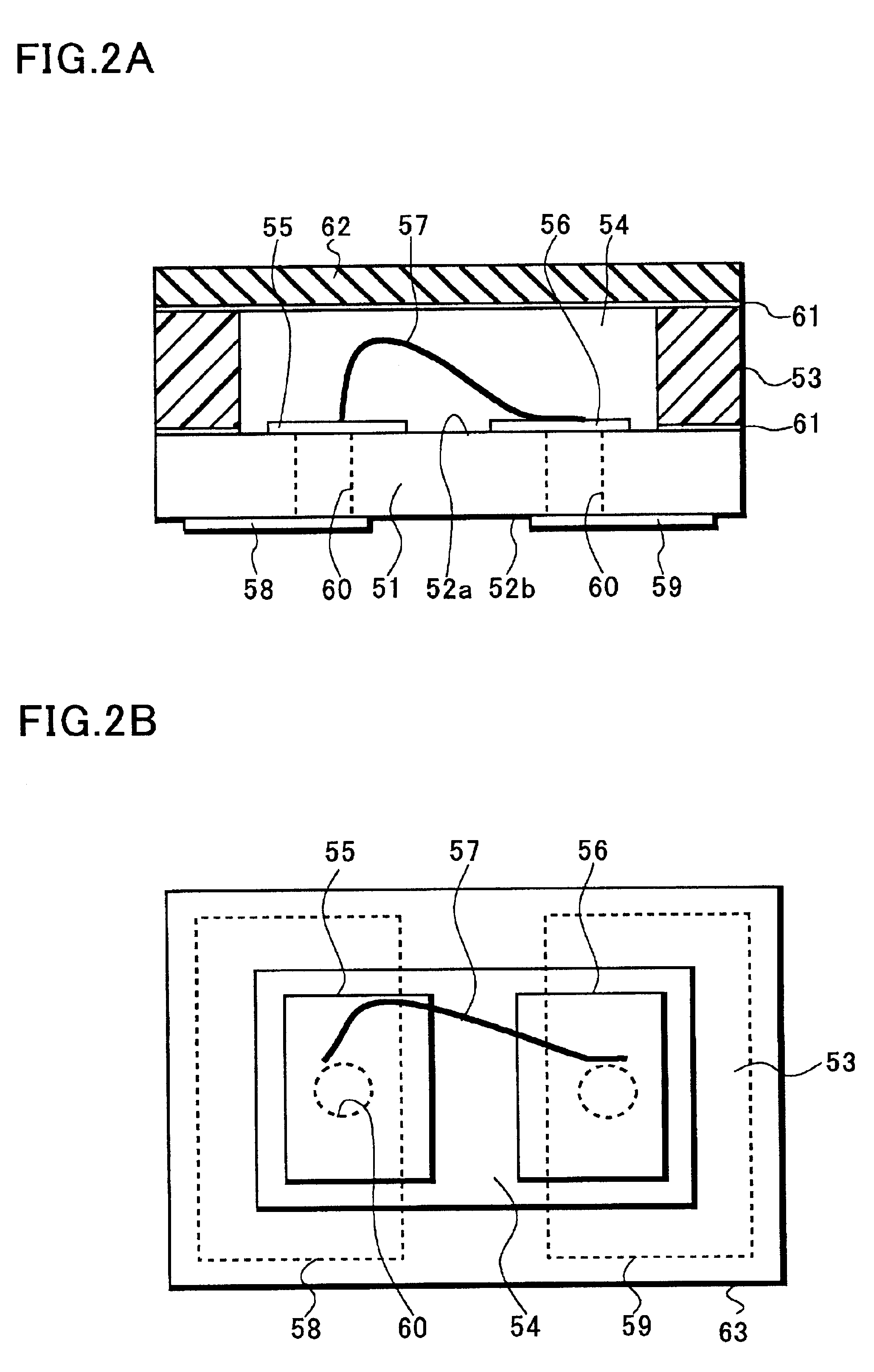
FIG. 1A is a sectional view and FIG. 1B is a plan view showing an embodiment of the semiconductor device of the present invention. A substrate 21a divided from a large-sized substrate 21 is formed of insulating material such as ceramic, glass epoxy, etc., and has a plate thickness of 100 to 300 μm and a rectangular shape whose long side×short side is about 2.5 mm×1.9 mm when it is viewed as a plan view (viewed as shown in FIG. 1B). Also, the substrate 21a has a first main face 22a on the surface side and a second main face 22b on the back surface side respectively, and these faces extend in parallel with each other. A column portion 23 is an pillar portion that is provided on an outer periphery of the substrate 21a to have a height of about 0.4 mm and a width of about 0.5 mm. A concave portion 24 is formed on the center portion of the substrate 21a by the column portion 23. Th...


PUM


Abstract

The present invention comprises a first main face (22a) on a surface side of a substrate (21a). An island portion (26) is formed on the first main face (22a) and a semiconductor chip (29), etc. are adhered thereto. The semiconductor chip (29), etc. are sealed in the hollow portion that is constructed by a column portion (23) and a transparent glass plate (36). Then, the column portion (23) and the transparent glass plate (36) are adhered by epoxy resin, or the like.

Description

BACKGROUND OF THE INVENTIONThe present invention relates to a semiconductor device that includes a semiconductor element for high frequency applications and an overcurrent-protecting function in a hollow airtight package and a method of manufacturing the same.An example of the semiconductor device employing the hollow package in the conventional art is shown in FIG. 9. This electronic parts comprise a base substrate 1 formed of ceramic, etc., a lead 2 for external connection, and a cap 3 formed similarly of ceramic. A semiconductor chip 5 is adhered onto a surface of an element mounting portion 4 of the lead 2, then the semiconductor chip 5 and the lead 2 are connected via bonding wires 6, and then the semiconductor chip 5 is sealed in an airtight space 7 constructed by the cap 3 (for example, Patent Application Publication Hei 10-173117).Such parts are manufactured via steps of preparing the lead 2 in the form of a lead frame, then bonding the semiconductor chip 5 to the lead frame...

Claims


Application Information

Patent Timeline
Patent Type & Authority Patents(United States)
IPC IPC(8): H01L23/02H01L23/58H01L23/055H01L23/10H01L23/62
CPCH01L23/055H01L23/62H01L24/97H01L23/10H01L2224/45144H01L2224/32225H01L2224/48091H01L2224/48227H01L2224/48247H01L2224/48257H01L2224/73265H01L2224/97H01L2924/01004H01L2924/01029H01L2924/01033H01L2924/01047H01L2924/01074H01L2924/01078H01L2924/01079H01L2924/01082H01L2924/09701H01L2924/13091H01L2924/16195H01L2924/19043H01L2924/01005H01L24/48H01L2924/12041H01L2924/1306H01L2924/12032H01L2224/85H01L2224/83H01L2924/00014H01L2924/00H01L2224/45015H01L24/45H01L2924/20753
Inventor HYODO, HARUOKIMURA, SHIGEOTAKANO, YASUHIRO
Owner SEMICON COMPONENTS IND LLC
Why Eureka
Try Eureka