Circuit module and manufacturing method thereof

A technology of circuit components and manufacturing methods, applied in circuits, semiconductor/solid-state device manufacturing, electrical components, etc., can solve the problems of reduced test efficiency, increased packaging area, and increased number of pins, saving pin space, The effect of reducing the package area and improving the yield

Pending Publication Date: 2018-08-24
HANGZHOU SILAN MICROELECTRONICS
View PDF0 Cites 8 Cited by
  • Summary
  • Abstract
  • Description
  • Claims
  • Application Information

AI Technical Summary

Problems solved by technology

However, it is disadvantageous for the dedicated test pins to be exposed in the final product, which not only leads to an increase in the number of pins and a corresponding increase in the package area, but also needs to be identified during use, resulting in inconvenience
If the test pin is wrongly connected in the final product, it may even cause chip damage
The use of dual-purpose test pins will cause excessive delays, resulting in reduced test efficiency

Method used


Image

  • Circuit module and manufacturing method thereof
  • Circuit module and manufacturing method thereof
  • Circuit module and manufacturing method thereof

Examples


Embodiment Construction

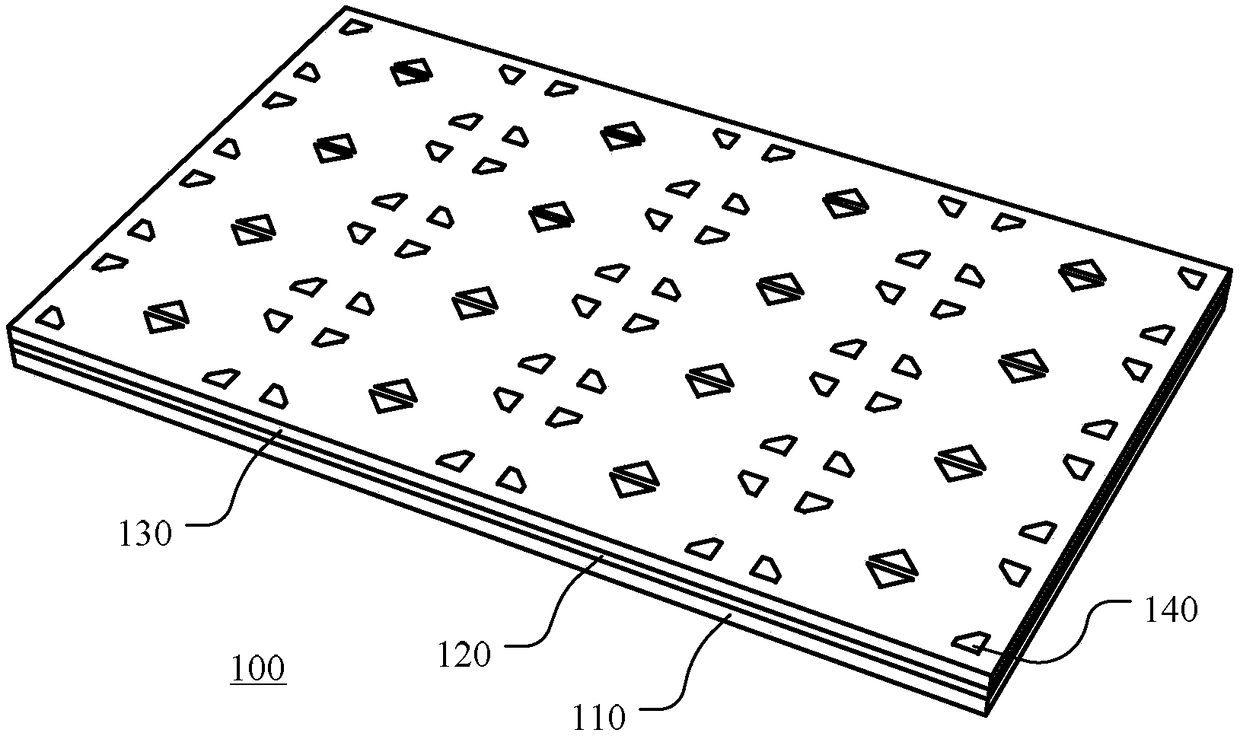
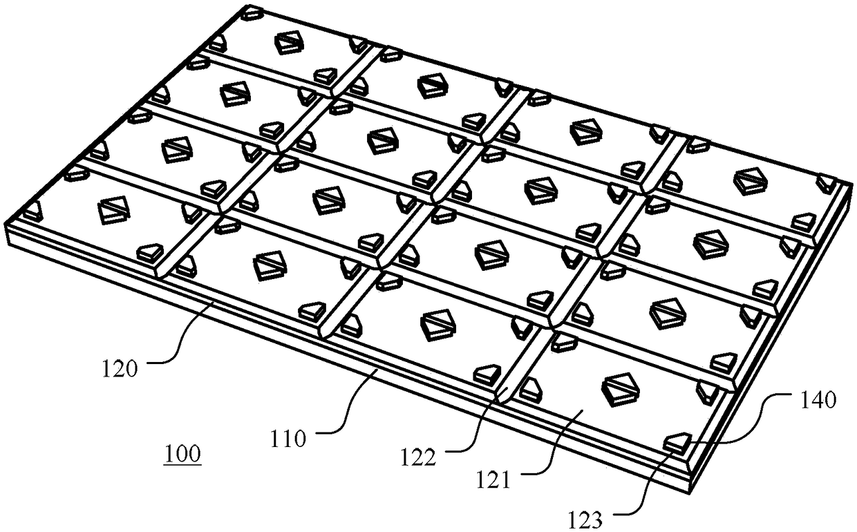
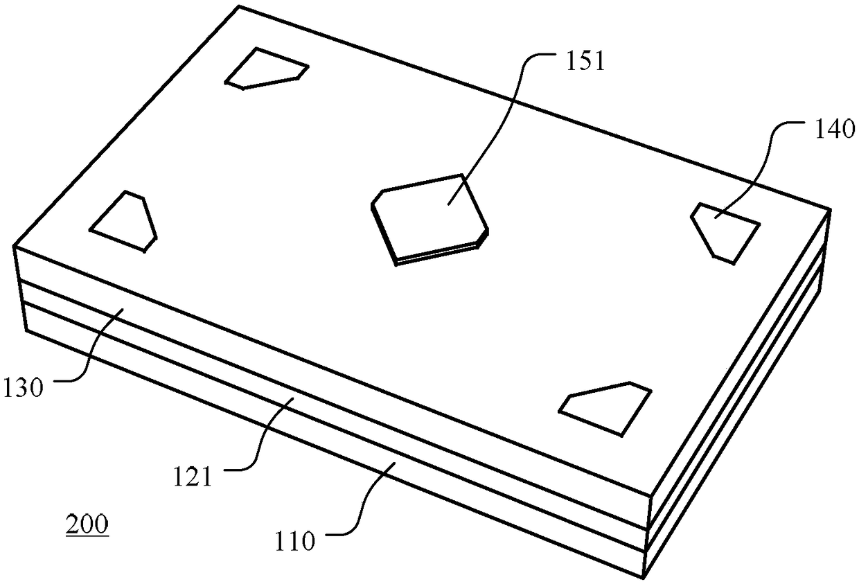
[0054] Hereinafter, the present invention will be described in more detail with reference to the accompanying drawings. In the various drawings, the same elements are represented by similar reference numerals. For the sake of clarity, the various parts in the drawings are not drawn to scale. In addition, some well-known parts may not be shown.

[0055] It should be understood that when describing a certain structure, when a layer or area is referred to as being "on" or "above" another layer or another area, it can mean directly on the other layer or area, or It also includes other layers or regions between it and another layer or another region. Moreover, if the structure is turned over, the layer or area will be "below" or "below" the other layer or area. If in order to describe the situation of being directly on another layer and another area, this article will adopt the expression "A directly on B" or "A on and adjacent to B".

[0056] In the description of the present inven...


PUM


Abstract

The invention discloses a circuit module and a manufacturing method thereof. The circuit module comprises a printed circuit board, a package chip and a switch tube, wherein the package chip and the switch tube are arranged on the printed circuit board, the package chip comprises a chip, a first plastic package layer and a plurality of metal posts, the first plastic package layer covers the chip, each metal post comprises a first end and a second which are opposite to each other, the first end is in contact with the chip, and the second end is exposed out of the first plastic package layer. Thepackage chip in the circuit module employs the metal posts to external electrical connection, so that the package area is reduced, and the reliability is improved.

Description

Technical field [0001] The present invention relates to the technical field of chip manufacturing, and more specifically, to a circuit assembly and a manufacturing method thereof. Background technique [0002] With the widespread application and rapid development of mobile terminals and consumer electronic products, charging protection chips for electronic products are becoming more and more important. The charging protection chip not only needs to meet the requirement of continuously reducing the area of ​​electronic products, but also needs to meet the requirements of fast charging to save charging time, and to meet the requirements of testing to screen out failed circuit chips. Therefore, the performance requirements for electronic products, especially lithium battery charging protection chips, are gradually increasing, the area of ​​the chip is gradually reduced, and the chip is required to have better heat dissipation to meet the demand for fast charging. This requires circ...

Claims


Application Information

Patent Timeline
Patent Type & Authority Applications(China)
IPC IPC(8): H01L23/488H01L23/31H01L23/367H01L21/50
CPCH01L2224/73104H01L24/14H01L21/50H01L23/3114H01L23/3677
Inventor 邱政胡铁刚潘华兵金沈阳
Owner HANGZHOU SILAN MICROELECTRONICS
Why Eureka
Try Eureka