Gold-wire-free encapsulation method of large power white light LED part and white light LED part

A technology for LED devices and packaging methods, which is applied in the direction of electric solid devices, semiconductor devices, electrical components, etc., can solve the problems affecting the injection efficiency and forward working voltage of LED devices, the large contact resistance between the gold wire and the chip contact point, the phosphor and the filling The problem of low thermal conductivity of the sealant can improve the light emitting efficiency of LEDs, solve the shortcomings of the gold wire process, and reduce the package area and package thickness.

Active Publication Date: 2010-10-13
KUSN KAIWEI ELECTRONICS
View PDF4 Cites 8 Cited by
  • Summary
  • Abstract
  • Description
  • Claims
  • Application Information

AI Technical Summary

Problems solved by technology

[0007] 2. The process of making gold wires on pn electrodes is cumbersome, high cost and low reliability:
[0009] 3. The contact resistance between the gold wire and the chip contact point is large, which affects the injection efficiency and forward working voltage of the LED device, causing the device to heat up, dec

Method used


Image

  • Gold-wire-free encapsulation method of large power white light LED part and white light LED part
  • Gold-wire-free encapsulation method of large power white light LED part and white light LED part
  • Gold-wire-free encapsulation method of large power white light LED part and white light LED part

Examples


preparation example Construction

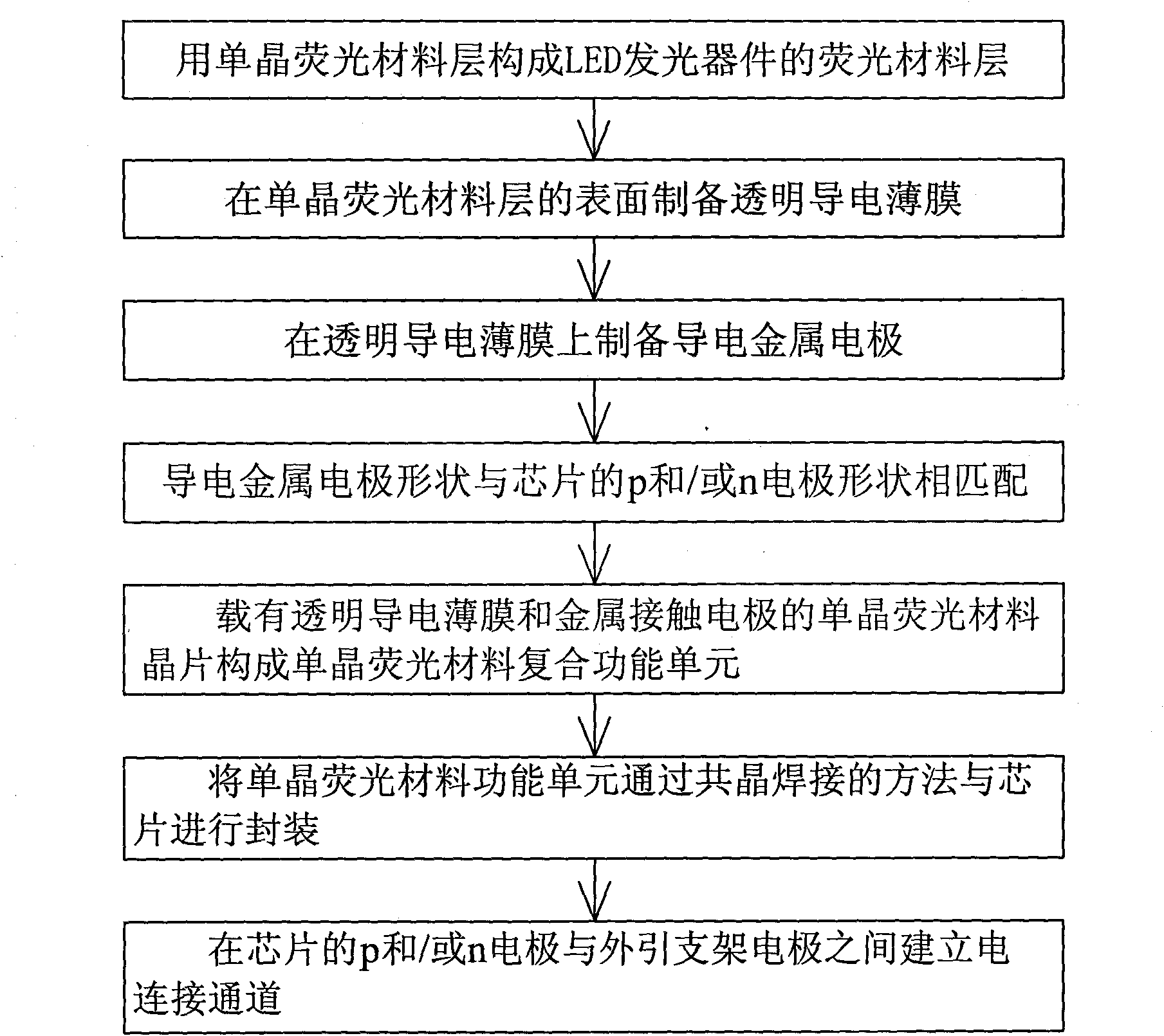
[0052] The preparation of the transparent conductive film and the conductive metal electrode adopts a photoetching method, a mask method, a laser dry etching method, a screen printing method or a through-mask deposition method.

[0053] Using transparent conductive films and conductive metal electrodes instead of gold wires for packaging can effectively increase the light-emitting area of ​​LED light-emitting chips, increase luminous flux, and improve LED light-emitting efficiency.

[0054]The above-mentioned transparent conductive film, conductive metal electrode and their preparation methods are all prior art, and their specific methods and processes will not be described here.

[0055] Furthermore, the single crystal fluorescent material functional unit is arranged on at least one side of the chip. As a special case, the single crystal fluorescent material functional unit can be arranged on two sides of the chip to form a double-sided light-emitting device.

[0056] The tr...

Embodiment 1

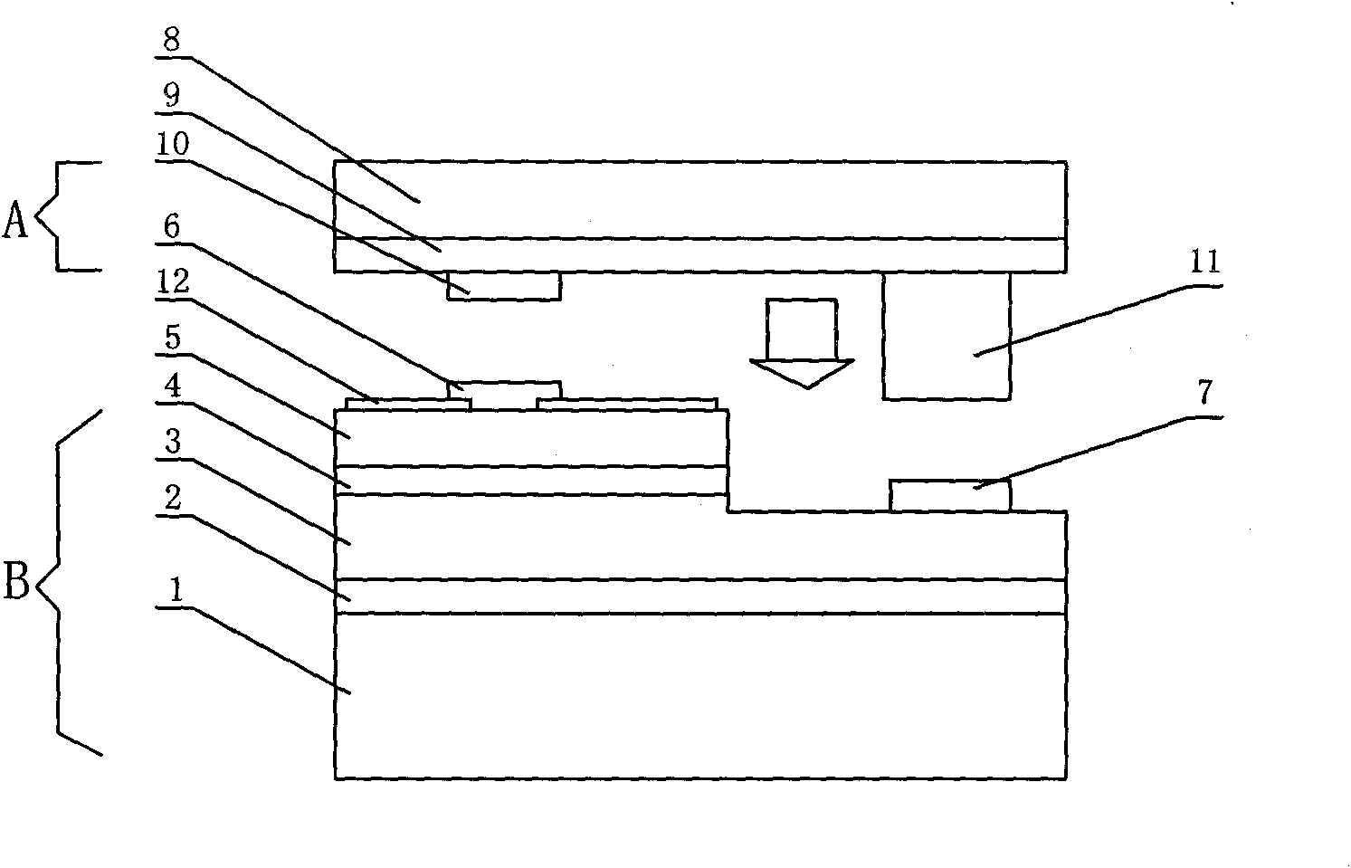
[0060] a use figure 1 The structure of the high-power white LED device manufactured by the packaging method is as shown.

[0061] figure 2 In the structure of conventional LED light-emitting chips, the buffer layer / u-GaN layer 2 is usually set on the substrate layer 1, followed by the n-GaN layer 3, the active region 4 and the p-GaN layer 5, and the n-GaN layer and the On the p-GaN layer, ohmic contact surfaces (ie commonly known as p and / or n electrodes) 6 and 7 for electrical connection and extraction are provided.

[0062] In this technical solution, at least one side of the LED light-emitting chip B is provided with a single crystal fluorescent material functional unit A composed of a single crystal fluorescent material layer 8, a transparent conductive film 9 and conductive metal electrodes 10 and 11 in sequence.

[0063] It can be seen from the figure that the single crystal fluorescent material functional unit forms an electrical connection channel between the pn jun...

Embodiment 2

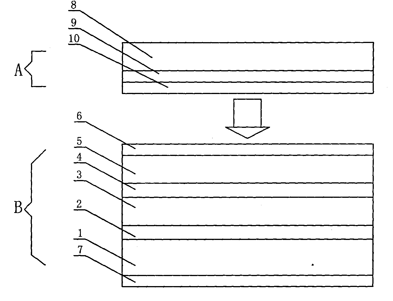
[0074] Another use figure 1 The high-power white light LED device that described encapsulating method manufactures, its structure is as follows image 3 shown.

[0075] image 3 Among them, the LED chip is a vertical structure (Vertical), and the two electrodes 6 and 7 of the vertical structure LED chip are respectively on both sides of the LED epitaxial layer (p-GaN layer 5 and n-GaN layer 3).

[0076] Similarly, when a single-crystal fluorescent material is used as the substrate layer 1 below the n-GaN structure layer 3 in the figure, an LED light-emitting device capable of truly double-sided light-emitting / light-emitting can be formed.

[0077] The rest are the same figure 1 or figure 2 mentioned.

[0078] After adopting the above-mentioned structure, multiple LED light-emitting chips can be arranged simultaneously on one base material by adopting a chip-on-board packaging method, which helps to improve the luminous quantity and luminous flux of a single LED light-emi...


PUM


Abstract

The invention relates to a gold-wire-free encapsulation method of a large power white light LED part and a white light LED part, which belong to the field of the semiconductor luminous part, and comprise a chip is electrically connected with an outer lead bracket electrode, a fluorescent material layer is arranged at one side of the chip, a mono-crystal fluorescent material layer is adopted to form the fluorescent material layer, a transparent conductive film is prepared on the surface of the mono-crystal fluorescent material layer, a conductive metal electrode is arranged on the transparent conductive film, a mono-crystal fluorescent material wafer which carries the transparent conductive film and the conductive metal electrode forms a mono-crystal fluorescent material composite-functionunit, the mono-crystal fluorescent material composite-function unit is encapsulated with the chip through an eutectic welding way, and an electric connection channel is established between a pn electrode of the chip and the outer lead bracket electrode. By adopting the surface contact-type electric connection, the encapsulation reliability of the white light LED part is improved, the service lifeof the LED is remarkably prolonged, and the light-emitting efficiency is improved. The method is particularly applicable to the mass integration encapsulation production process and can effectively reduce the manufacturing cost of the LED luminous part.

Description

technical field [0001] The invention belongs to the field of semiconductor light-emitting devices, and in particular relates to a packaging method for high-power white LED devices and a product structure thereof. Background technique [0002] In the existing LED (Light Emitting Diode, light-emitting diode) manufacturing technology, the packaging of LED light-emitting devices is usually to make pn junction electrodes on the blue light chip, and to make gold wires on the electrodes (the gold wires are used to connect the LED chip and external wiring. The connection wire of the pin), connect the chip electrode to the external pin, and then coat the phosphor on the chip. [0003] A Chinese invention patent application with a publication date of November 8, 2006 and a publication number of CN 1858920A "A Packaging Method for White Light LED Lamps" and a Chinese invention patent application with a publication date of August 26, 2009 and a publication number of CN 101514805A In th...

Claims


Application Information

Patent Timeline
IPC IPC(8): H01L33/48H01L33/62H01L33/50H01L33/42
CPCH01L2224/14
Inventor 李思兰杨莹胡泉
Owner KUSN KAIWEI ELECTRONICS
Why Eureka
Try Eureka