Solar silicon wafer processing method and device

A technology of solar silicon wafers and processing methods, applied to fine working devices, stone processing equipment, working accessories, etc., to achieve the effect of reducing labor intensity and improving production capacity

Inactive Publication Date: 2014-01-22
INNER MONGOLIA ZHONGHUAN SOLAR MATERIAL
View PDF10 Cites 2 Cited by
  • Summary
  • Abstract
  • Description
  • Claims
  • Application Information

AI Technical Summary

Problems solved by technology

This method adopts the improvement of the material seat, so that the material plate and the material seat are degummed at the same time; because the weight of the material plate and the material seat is relatively large, the mechanical arm is used instead of manual handling; the material plate and the material seat are placed in the boiling water at the same time. The method of boiling water in the box ensures that the material board and the material seat are always connected together during the processing, thus solving the problem that the material board and the material seat are disassembled, processed separately, and then reinstalled, so as to improve production efficiency. The purpose of increasing economic benefits

Method used


Image

  • Solar silicon wafer processing method and device
  • Solar silicon wafer processing method and device
  • Solar silicon wafer processing method and device

Examples


Embodiment Construction

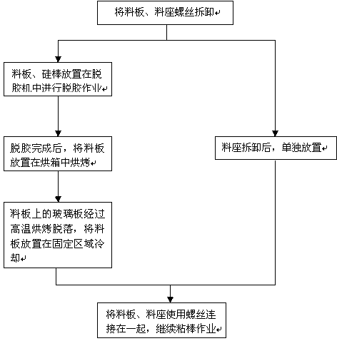
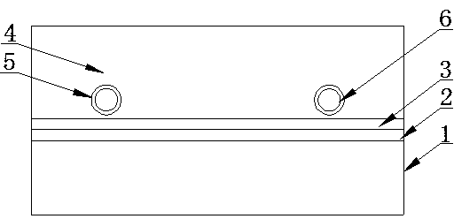
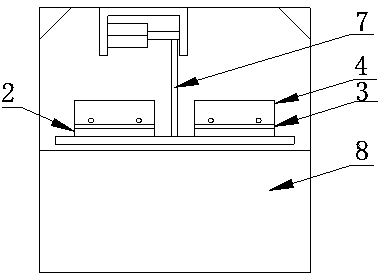
[0012] The present invention will be further described below with reference to accompanying drawing: figure 2 , image 3 and Figure 4 , a kind of solar silicon chip processing method concrete steps are as follows:

[0013] (1) First, drill two through holes 5 in the lower part of the side of the material seat 4, and then carry out the sticking operation (glue the solar silicon rod 1, the glass plate 2, and the material plate 3, and fix the material plate 3 and the material seat 4 with screws) .

[0014] (2) After cutting the solar silicon rods with a wire cutting machine, insert two metal round rods 6 into the two through holes 5 on the side of the material holder 4 (such as figure 2 shown), the two ends of the two metal round rods 6 protrude from the two through holes 5 on the side of the material seat 4 respectively, and the operator uses the two metal round rods 6 to place the solar silicon rod 1, the glass plate 2, and the material plate 3 Together with the material...


PUM


Abstract

The invention relates to a solar silicon wafer processing method and device. First, two through holes are formed in a material base, and then rod gluing operation is conducted; after a solar silicon rod is cut, two round metal rods are inserted in the two round holes in the material base respectively, and the solar silicon rod, a glass plate, a material plate and the material base are integrally placed in a skip car of a degumming machine together through the two round metal rods; a solar silicon wafer falls off through a degumming process, and a mechanical arm is used for integrally placing the glass plate, the material plate and the material base in a water boiling box together; the glass plate on the material plate falls off through water boiling, and then the mechanical arm is used for transporting the material plate and the material base back to a rod gluing table integrally; rod gluing operation continues to be conducted after the material plate and the material base are cooled. Due to the fact that the material plate and the material base are connected together all the time in the whole processing process, the problems that work hours are wasted and processing quality has hidden dangers as a result of frequent dismounting and mounting of the material plate and the material base are effectively avoided, labor intensity of manpower is lowered, and production capacity of the solar silicon wafer is improved.

Description

technical field [0001] The invention relates to the optimization of solar silicon wafer processing technology, in particular to a solar silicon wafer processing method and device. Background technique [0002] In the solar energy industry, the transfer method of the material sheet and the material holder is basically to disassemble the material holder before the degumming process, and place the material holder separately. After the degumming process, place the material sheet in an oven to bake until the glass on the material sheet The plate falls off, and after the temperature of the material plate is cooled, the method of reinstalling the material plate and the material seat is as follows: figure 1 shown. Using this method will usually lead to three situations: ①When degumming, the material seat is disassembled and placed separately, which takes up space; ②Frequent disassembly and installation of the material plate and material seat will increase the production labor; ③Fre...

Claims


Application Information

Patent Timeline
Patent Type & Authority Applications(China)
IPC IPC(8): B28D5/00B28D7/00
Inventor 白建军王若飞王贵龙章明远李兵兵武瑞
Owner INNER MONGOLIA ZHONGHUAN SOLAR MATERIAL
Why Eureka
Try Eureka