Three-dimensional ultrasonic imaging area array probe wiring method and three-dimensional ultrasonic imaging device

A technology of three-dimensional ultrasound and wiring method, which is applied in the directions of ultrasound/sonic wave/infrasonic wave diagnosis, acoustic wave diagnosis, infrasonic wave diagnosis, etc., to achieve the effect of improving electrical conductivity, simple operation, and good imaging effect

Inactive Publication Date: 2014-01-29
HUAZHONG UNIV OF SCI & TECH
View PDF8 Cites 7 Cited by
  • Summary
  • Abstract
  • Description
  • Claims
  • Application Information

AI Technical Summary

Problems solved by technology

[0005] In view of the above defects or improvement needs of the prior art, the present invention provides a wiring method for a three-dimensional ultrasonic imaging area array probe and a three-dimensional ultrasonic imaging device using the wiring method. The array elements are firmly connected and have good conductivity between the signal line and the 3D ultrasound imaging area array probe, thus solving the problems of the current 3D ultrasound imaging area array probes caused by mismatched wiring accuracy or weak wiring. To solve the technical problem of high defective rate, so as to provide a mass-produced three-dimensional ultrasonic imaging device using a three-dimensional ultrasonic imaging area array probe

Method used


Image

  • Three-dimensional ultrasonic imaging area array probe wiring method and three-dimensional ultrasonic imaging device
  • Three-dimensional ultrasonic imaging area array probe wiring method and three-dimensional ultrasonic imaging device
  • Three-dimensional ultrasonic imaging area array probe wiring method and three-dimensional ultrasonic imaging device

Examples


Embodiment 1

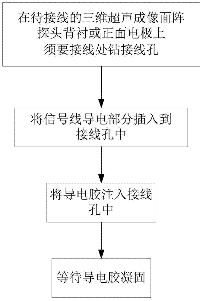
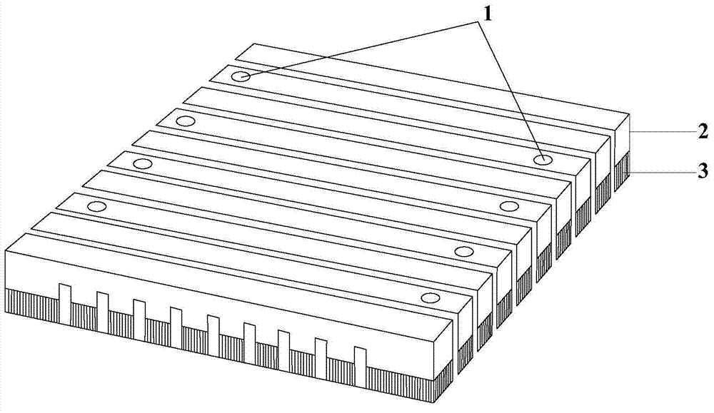
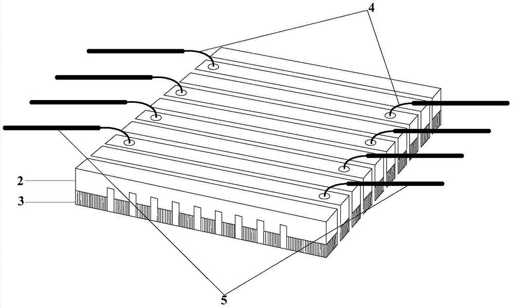
[0046] The backing of the three-dimensional ultrasonic imaging area array probe is cut into 8 columns by mechanical cutting, each column corresponds to 8 transducer units, the array width is about 120 microns, and the array spacing is about 45 microns. The material used is E-solder3022.

[0047] Under the microscope, use a thin wire needle with a diameter of about 80 microns to drill wiring holes at the required line of the backing array of the three-dimensional ultrasound imaging area array probe. In order to reduce the difficulty of wiring, the wiring holes are drilled at odd-even intervals. First, select 1, 3, and 5 odd-numbered columns to drill wiring holes on one side of the 3D ultrasound imaging area array probe backing array, and then select 2, 4, and 6 on the other side. Drill wiring holes in even rows. In this way, the drilled wiring holes are evenly distributed on both sides of the backing array of the three-dimensional ultrasonic imaging area array probe. Such as ...

Embodiment 2

[0052] The three-dimensional ultrasound imaging area probe is a front piezoelectric sheet (PZT) that is cut into an 8*8 matrix by mechanical cutting, with 8 transducer units in each row and column, and a total of 64 transducer units. The width of the transducer unit is about 120 microns, and the distance between the transducer units is about 45 microns. The electrodes covering the front array are gold electrodes, which are connected to the holes drilled in the front array by means of metal needles with a diameter of about 60 microns. .

[0053] Under a microscope, wiring holes are drilled in the piezo-electric (PZT) array using thin wire-type needles with a diameter of approximately 80 microns. In order to reduce the difficulty of wiring, the wiring holes are drilled at odd-even intervals. First, select 1, 3, and 5 odd-numbered columns to drill wiring holes on one side of the piezoelectric film (PZT) array, and then select 2, 4, and 6 even-numbered columns on the other side. ...

Embodiment 3

[0058] The wired three-dimensional ultrasound imaging area probe in embodiment 1 or embodiment 2 is connected with the corresponding conversion circuit and computer, and assembled into a three-dimensional ultrasound imaging device.


PUM


Abstract

The invention discloses a three-dimensional ultrasonic imaging area array probe wiring method and a three-dimensional ultrasonic imaging device. The three-dimensional ultrasonic imaging area array probe wiring method and the three-dimensional ultrasonic imaging device aim to solve the problems that according to an existing three-dimensional ultrasonic imaging area array probe wiring method, the defective rate is high and wiring is not firm. According to the three-dimensional ultrasonic imaging area array probe wiring method and the three-dimensional ultrasonic imaging device, a wiring hole is firstly drilled in a wiring position of a three-dimensional ultrasonic imaging area array probe, then the conductive part of a signal line is inserted into the wiring hole, conductive adhesive is then poured into the wiring hole treated in last step, and finally wiring is achieved after the conductive adhesive is solidified. The three-dimensional ultrasonic imaging device is formed by connection of the three-dimensional ultrasonic imaging area array probe and a corresponding switching circuit and computer with the wiring method. The three-dimensional ultrasonic imaging area array probe wiring method and the three-dimensional ultrasonic imaging device have the advantages that the signal line can be connected firmly, the conduction performance is good, requirements of mechanical cutting accuracy can be met, and the defective rate is low during production. The three-dimensional ultrasonic imaging area array probe wiring method and the three-dimensional ultrasonic imaging device are applicable to micron-sized three-dimensional ultrasonic imaging area array probes.

Description

technical field [0001] The invention belongs to the field of three-dimensional ultrasonic imaging, and more specifically relates to a wiring method for a three-dimensional ultrasonic imaging area array probe and a three-dimensional ultrasonic imaging device using the wiring method. Background technique [0002] Ultrasound imaging technology is non-destructive, cheap, and convenient, and it is an important diagnostic imaging method in clinical medicine today. Because it can present real-time stereoscopic images of human tissues and organs, 3D ultrasound imaging technology has attracted people's attention. The core of 3D ultrasound imaging technology is the area array probe, and the difficulty of the area array probe lies in the wiring of the array elements. [0003] There are two wiring methods for 3D ultrasound imaging area array probes: full wiring and array wiring. For the three-dimensional ultrasonic imaging area probe with N×N array elements, the full wiring method mea...

Claims


Application Information

Patent Timeline
Patent Type & Authority Applications(China)
IPC IPC(8): A61B8/00
Inventor 朱本鹏孙士越张悦陈实杨晓非
Owner HUAZHONG UNIV OF SCI & TECH
Why Eureka
Try Eureka