Substrate inspection device and transmission illumination device for substrate inspection device

A substrate inspection and substrate technology, which is applied in the direction of optical testing flaws/defects, etc., can solve the problems of high infrared light intensity, difficulty in identification, and inability to accurately identify microcracks or pores in solar cells, so as to improve uniformity and low cost. Effect

Inactive Publication Date: 2016-11-02
SHIMADZU SEISAKUSHO CO LTD
View PDF7 Cites 0 Cited by
  • Summary
  • Abstract
  • Description
  • Claims
  • Application Information

AI Technical Summary

Problems solved by technology

[0005] In this substrate inspection device, when the infrared light irradiated from the light source passes through the outside of the edge of the substrate and directly enters the camera without passing through the substrate, compared with the infrared light that enters the camera after passing through the substrate, it directly enters the camera. The intensity of the infrared light is extremely high, so the image captured by the camera becomes extremely bright near the edge of the substrate, making it difficult to recognize the infrared light transmitted through the substrate
Therefore, it is impossible to accurately identify microcracks, pores, etc. that occur inside the solar cell.

Method used


Image

  • Substrate inspection device and transmission illumination device for substrate inspection device
  • Substrate inspection device and transmission illumination device for substrate inspection device
  • Substrate inspection device and transmission illumination device for substrate inspection device

Examples


Embodiment Construction

[0069] In order to further explain the technical means and effects of the present invention to achieve the intended purpose of the invention, the specific implementation methods of the substrate inspection device and the transmissive illumination device for the substrate inspection device proposed according to the present invention will be described below in conjunction with the accompanying drawings and preferred embodiments. , structure, feature and effect thereof, detailed description is as follows.

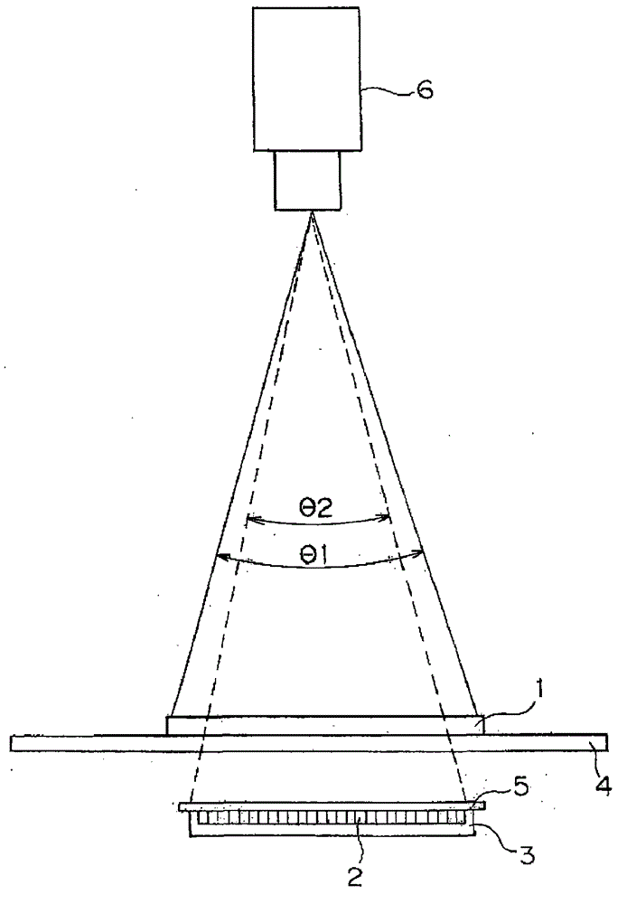
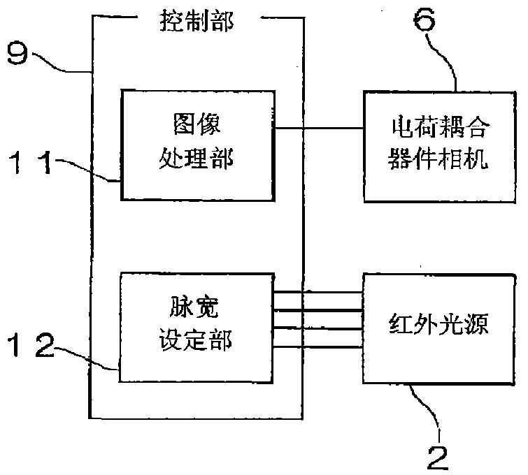
[0070] Hereinafter, a first embodiment of the present invention will be described based on the drawings. figure 1 It is a schematic diagram which shows the structure of the board|substrate inspection apparatus of this invention. also, figure 2 It is a block diagram (block diagram) showing the main control system of the board|substrate inspection apparatus of this invention. also, Figure 7 It is a schematic diagram showing the configuration of a conventional substrate insp...


PUM


Abstract

The invention relates to a substrate inspection device and a transmission illuminating device for the substrate inspection device. The substrate inspection device can prevent infrared light from an infrared light source from entering a camera without passing through the substrate, so that the substrate can be accurately inspected. The shape and arrangement of the infrared light source are set so that the field of view of the infrared light source of the charge-coupled device camera is covered by the field of view of the substrate of the charge-coupled device camera. Furthermore, by virtue of the Fresnel lens, the irradiation angle of the infrared light emitted from the light emitting diode element disposed near the edge of the infrared light source is deviated toward the edge direction of the substrate. In addition, the intensity of the infrared light irradiated from the infrared light source to the substrate on the edge region of the substrate is greater than the intensity of the infrared light on the central portion of the substrate.

Description

technical field [0001] The present invention relates to a substrate inspection device and a transillumination device for the substrate inspection device, and in particular to a substrate inspection device and a transillumination device for the substrate inspection device that use a substrate for a solar cell unit as an inspection object. Background technique [0002] Inspecting the shape of a fracture or a defect is performed on a substrate for a solar cell in a step before an electrode formation step in a manufacturing step of a solar cell, such as a receiving inspection step or a film-forming step of an antireflection film or after a film-forming step Inspection, inspection of particles attached to the substrate, pinholes of the anti-reflection film, surface condition inspection of uneven film thickness of the anti-reflection film, and inspection of microcracks generated inside the solar cell ( microcrack) or void (void) etc. internal inspection. [0003] Among them, when...

Claims


Application Information

Patent Timeline
Patent Type & Authority Patents(China)
IPC IPC(8): G01N21/88
Inventor 桥本丰之永井正道平出雅人纲泽义夫
Owner SHIMADZU SEISAKUSHO CO LTD
Why Eureka
Try Eureka