Power device and assembling method thereof

A technology of power devices and assembly methods, which is applied in the electronic field, can solve problems such as the decline of thermal conductivity and grounding performance, achieve the effects of improving heat dissipation performance and grounding performance, improving product performance indicators, and reducing packaging steps

Inactive Publication Date: 2014-02-05
HUAWEI TECH CO LTD
View PDF4 Cites 2 Cited by
  • Summary
  • Abstract
  • Description
  • Claims
  • Application Information

AI Technical Summary

Problems solved by technology

[0006] The embodiment of the present application provides a power device and a power device assembly method to solve the technical problem in the prior art that the heat conduction efficiency and grounding performance of the assembled product are reduced due to the use of packaged devices for assembly.

Method used


Image

  • Power device and assembling method thereof
  • Power device and assembling method thereof
  • Power device and assembling method thereof

Examples


Embodiment 1

[0063] Embodiment one, for image 3 Assembly process of medium power devices:

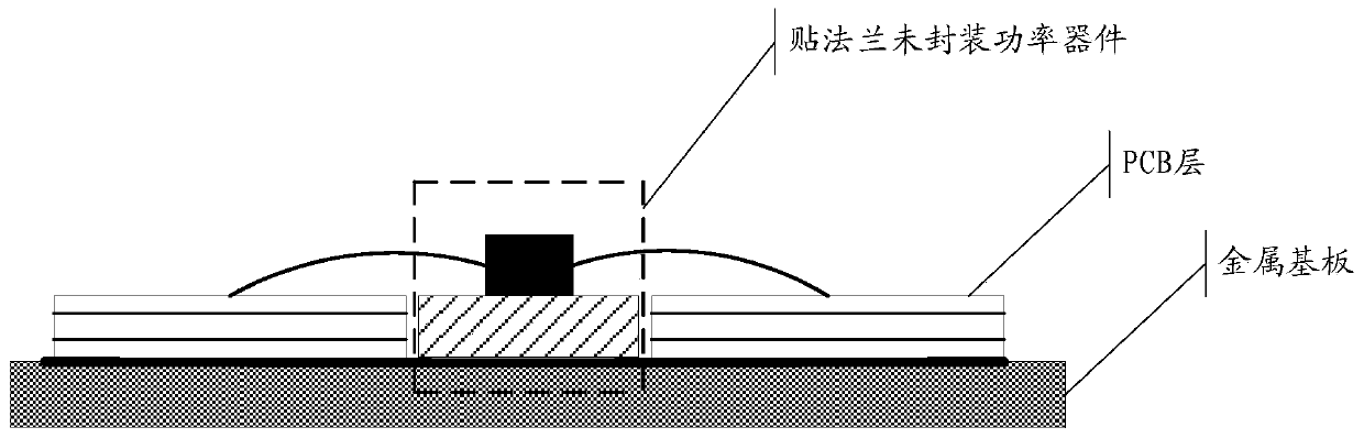
[0064] Executing step S1 is divided into two small steps: firstly, the metal medium 10 is embedded in the PCB layer 100, and then the PCB layer 100 embedded with the metal medium 10 is welded on the metal substrate 200, and the welding process is between the PCB layer 100 and the metal substrate. 200 to form a solder layer 40 .

[0065] Then step S2 is executed to arrange at least one bare chip 20 in the metal medium 10. In practical applications, S2 has two implementation methods. The first is to paste at least one bare chip 20 on the surface of the metal medium 10 with tin printing. The second is to provide at least one groove on the metal medium 10, paste the bare chip 20 after printing tin in the groove, wherein the number of the groove is the same as the number of the bare chip, and the bare chip can also be pasted. At the same time, low CTE solder is used to slow down the mismatch problem a...

Embodiment 2

[0068] Embodiment two, for Figure 4 Assembly process of medium power devices:

[0069] In the specific implementation process, step S1 is executed, and the metal medium 10 is first embedded in the metal substrate 200. Since the PCB layer 100 is to be welded on the metal substrate 200, the embedded metal medium 10 should protrude a part of the metal substrate 200; Then the PCB layer 100 is soldered and laid around the metal medium 10 , and the height of the installed PCB layer 100 is consistent with the height formed by the metal medium 10 . Then, as in the first embodiment, step S2 and step S3 are performed to form a power device.

Embodiment 3

[0070] Embodiment three, for Figure 5 Assembly process of medium power devices:

[0071] What is provided in this embodiment is an assembly method that directly uses the metal substrate 200 to form a metal medium for setting bare chips. Step S1 is performed to directly design the metal substrate 200 into a convex shape, and the metal boss on it can be used as The metal medium 10 of the bare chip is set, and then the PCB layer 100 is soldered around the metal boss by the same means as in the second embodiment, and the height of the PCB layer 100 is consistent with the metal boss (that is, the metal medium 10 ). Finally, steps S2 and S3 are performed to form a complete power device.

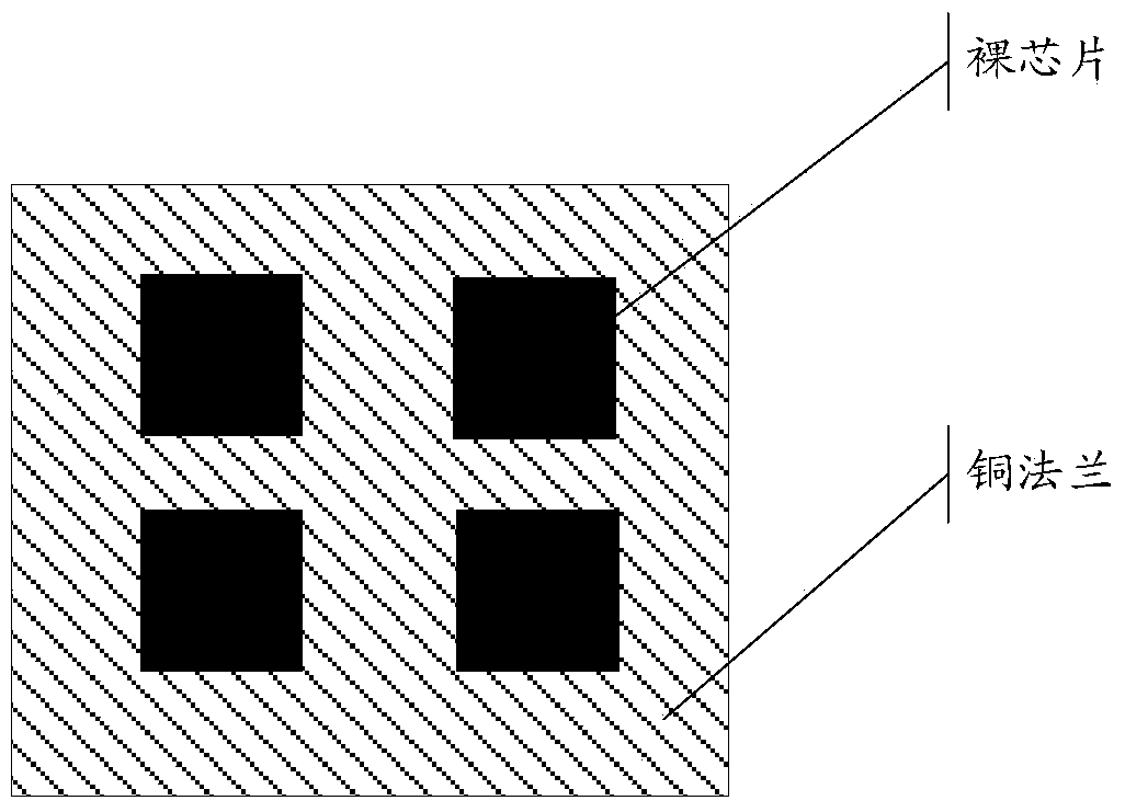
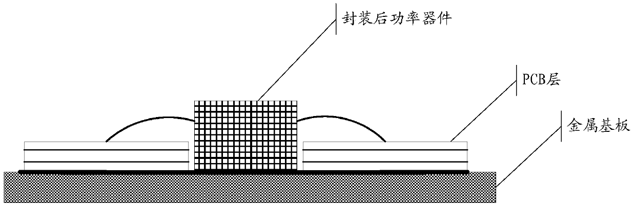
[0072] It can be seen from the assembly schemes in the above three embodiments that no matter which assembly method is used, the surface of the completed power device is the same, as Figure 7 as shown, Figure 7 It is a top view of the surface of the power device assembled through the above-me...


PUM


Abstract

The invention discloses a power device and an assembling method of the power device. The power device comprises metal media, at least one device body and at least one unpacked chip, the metal media are arranged in a substrate to be assembled, the at least one device body is arranged on the substrate to be assembled, the at least one unpacked chip is arranged on the metal media, and the at least one unpacked chip is electrically connected with the at least one device body.

Description

technical field [0001] The present application relates to the field of electronic technology, in particular to a power device and an assembly method of the power device. Background technique [0002] With the rapid development of the PCBA manufacturing process, at present, the PCBA assembly method is mainly based on the assembly of the device (bare die) with package form, and the casting plastic package or bonded ceramics are added outside the bare die as protection. This form is called Packaged devices; the existing PCBA process is roughly: by first welding the bare die to the copper flange, and then welding the flange to the metal product (PCBA / metal plate), when the bare die is welded to the copper flange , The surface is cast in plastic or pasted with a ceramic cover. [0003] Such as figure 1 as shown, figure 1 Shown is an electronic component used in the existing assembly scheme. By assembling the bare die on the metal flange or casting plastic or pasting ceramics, ...

Claims


Application Information

Patent Timeline
Patent Type & Authority Applications(China)
IPC IPC(8): H01L21/50H01L21/60H01L23/495H01L23/31
Inventor 丁丽蒋然何大鹏
Owner HUAWEI TECH CO LTD
Why Eureka
Try Eureka