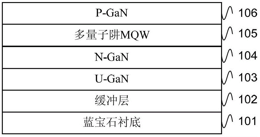
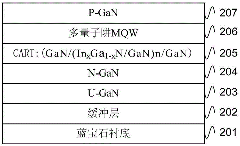
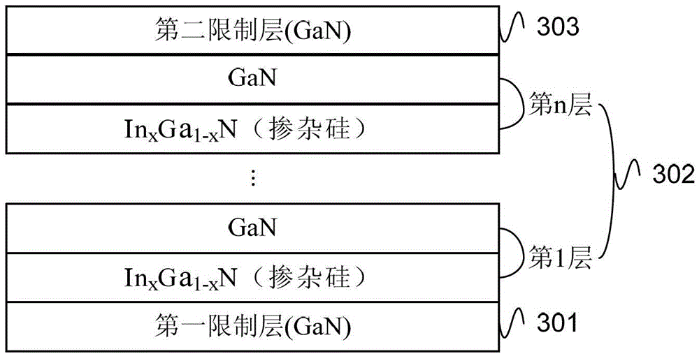
led epitaxial structure
An epitaxial structure and structure layer technology, applied in electrical components, circuits, semiconductor devices, etc., can solve the problems of PN junction breakdown, small distance, LED failure, etc., to achieve extended service life, reduced failure rate, reliability high effect
- Summary
- Abstract
- Description
- Claims
- Application Information
AI Technical Summary
Problems solved by technology
Method used
Image
Examples
Embodiment 1
[0015] 1. Put a patterned (PatternedSapphireSubstrate, PSS) sapphire substrate (which can be a substrate of other materials such as GaN) 201 into the reaction chamber, N 2 :H 2 : NH 3 The flow rate ratio is (0:120:0) SLM, the reaction chamber pressure is 500Torr, the temperature is raised to 1080°C, the rotation speed is 1200 (rev / s), and it is stable for 300s, and the substrate is purified at high temperature.
[0016] 2. Reduce the temperature to 540°C, the ratio of N2:H2:NH3 is (75:150:56) SLM, the pressure of the reaction chamber is controlled at 500 Torr, the rotation speed is 600 (rev / s), and a 35nm thick low-temperature GaN buffer layer 202 is grown.
[0017] 3. Raise the temperature to 1080°C, the ratio of N2:H2:NH3 is (75:150:56) SLM, the pressure of the reaction chamber is controlled at 200Torr, the speed is 1200 (rev / s), and a high-temperature non-doped material with a thickness of 1000nm is grown GaN layer (U-GaN) 203 .
[0018] 4. Keep the temperature at 1050°C...
PUM
 Abstract
Description
Claims
Application Information


