Calibration method of optical constant of metals and semiconductor thin film materials

A technology of optical constants and calibration methods, used in color/spectral characteristic measurement, measurement device, scattering characteristic measurement, etc., can solve the problems of low precision in the process of solving parameters and inability to judge the correct solution, and achieves wide applicability, elimination of error, the effect of improving accuracy and speed

Active Publication Date: 2014-02-12
DALIAN INST OF CHEM PHYSICS CHINESE ACAD OF SCI
View PDF15 Cites 16 Cited by
  • Summary
  • Abstract
  • Description
  • Claims
  • Application Information

AI Technical Summary

Problems solved by technology

However, the error of the theoretical calculation model itself and too many solution parameters make the accuracy of the solution process extremely low
figure 1 The solution space obtained when solving the optical

Method used


Image

  • Calibration method of optical constant of metals and semiconductor thin film materials
  • Calibration method of optical constant of metals and semiconductor thin film materials
  • Calibration method of optical constant of metals and semiconductor thin film materials

Examples


Embodiment 1

[0030] Embodiment 1: Calibration of optical constants of electron beam evaporated Cr film

[0031] 1. According to the method mentioned above, the optical constants of Cr thin films evaporated by electron beams were calibrated. We prepared thin film samples with an estimated physical thickness of 15-100 nm, and deposited them on BK7 optical glass at a deposition rate of 0.2 nm / s.

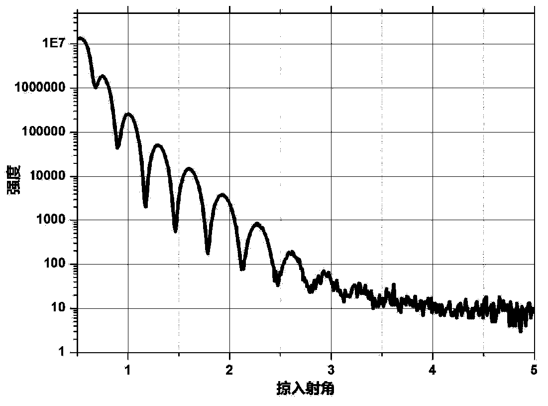
[0032] 2. The X-ray small-angle reflectance curve was tested for the film sample, and the X-ray with a wavelength of 0.154nm was selected for testing. Test curve such as figure 2 shown.

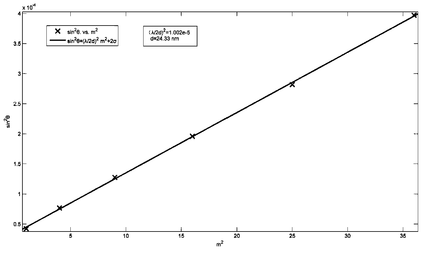
[0033] 3. According to the modified Bragg equation sin 2 θ m =(λ / 2d) 2 m 2 +2δ, λ=0.154nm Statistical data are shown in Table 1, and then do linear regression analysis, such as image 3 As shown, the thickness of the obtained film is 24.32 nm.

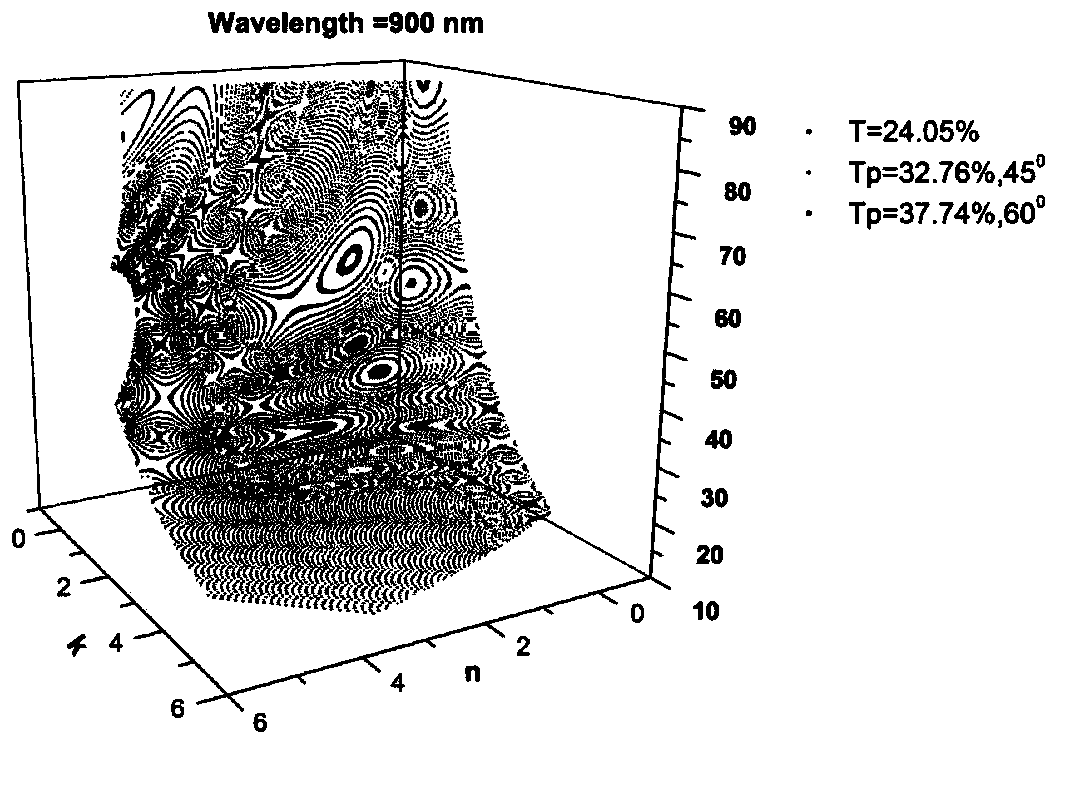
[0034] 4. The transmittance and reflectance values ​​of the test film at 0 degrees are shown in Table 2, and the test wavelength is from 415nm to 800nm.

[0035] 5...


PUM


Abstract

The invention relates to a method capable of precisely calibrating optical constant of metals and semiconductor thin film materials. The method is applicable to thin film state metals and semiconductor materials prepared by any processes. The method comprises the following steps: preparing a thin film sample with the thickness of 15-100nm; precisely calibrating the thickness by an X-ray total reflection spectrum method; testing a transmissivity spectral line and a reflectivity spectral line; and solving the optical constant by a graphical method. Compared with conventional spectrum direct analyzing method, the method provided by the invention can solve the problem of precisely solving the thickness of metals and semiconductor thin films, reduces the error caused by inability of precisely calibrating the thickness, simplifies the solving process and improves the solving precision and speed of the optical constant. The method has wide applicability and can provide accurate reference data to all scientific and engineering problems related to the optical constant of the metals and semiconductor thin film materials.

Description

technical field [0001] The invention relates to the field of basic research on the application of thin film materials, in particular to a calibration method for optical constants of metal and semiconductor thin film materials. Background technique [0002] Optical constants (N=n-k*i) are one of the basic properties of materials. The calibration of optical constants of thin film materials is the prerequisite for the optical application of such materials. Metal and semiconductor thin film materials are widely used in various fields, such as thin film solar cells, photothermal selective films, LED chip design, etc. In these specific applications, the premise of thin film structure design is to accurately calibrate the optical constants of the material. However, since metals and semiconductors are strong absorbing materials, the imaginary part k of their optical constants is not equal to 0, and there is one more unknown in the solution process than dielectric materials, which ...

Claims


Application Information

Patent Timeline
IPC IPC(8): G01N21/25G01N21/55G01B15/02
Inventor 邓淞文李刚孙龙
Owner DALIAN INST OF CHEM PHYSICS CHINESE ACAD OF SCI
Why Eureka
Try Eureka