Non-volatile memory device with clustered memory cells

A memory cell, non-volatile technology, used in static memory, read-only memory, digital memory information, etc.

Active Publication Date: 2014-02-12
STMICROELECTRONICS SRL
View PDF4 Cites 3 Cited by
  • Summary
  • Abstract
  • Description
  • Claims
  • Application Information

AI Technical Summary

Problems solved by technology

This need leads to specific array designs

Method used


Image

  • Non-volatile memory device with clustered memory cells
  • Non-volatile memory device with clustered memory cells
  • Non-volatile memory device with clustered memory cells

Examples


Embodiment Construction

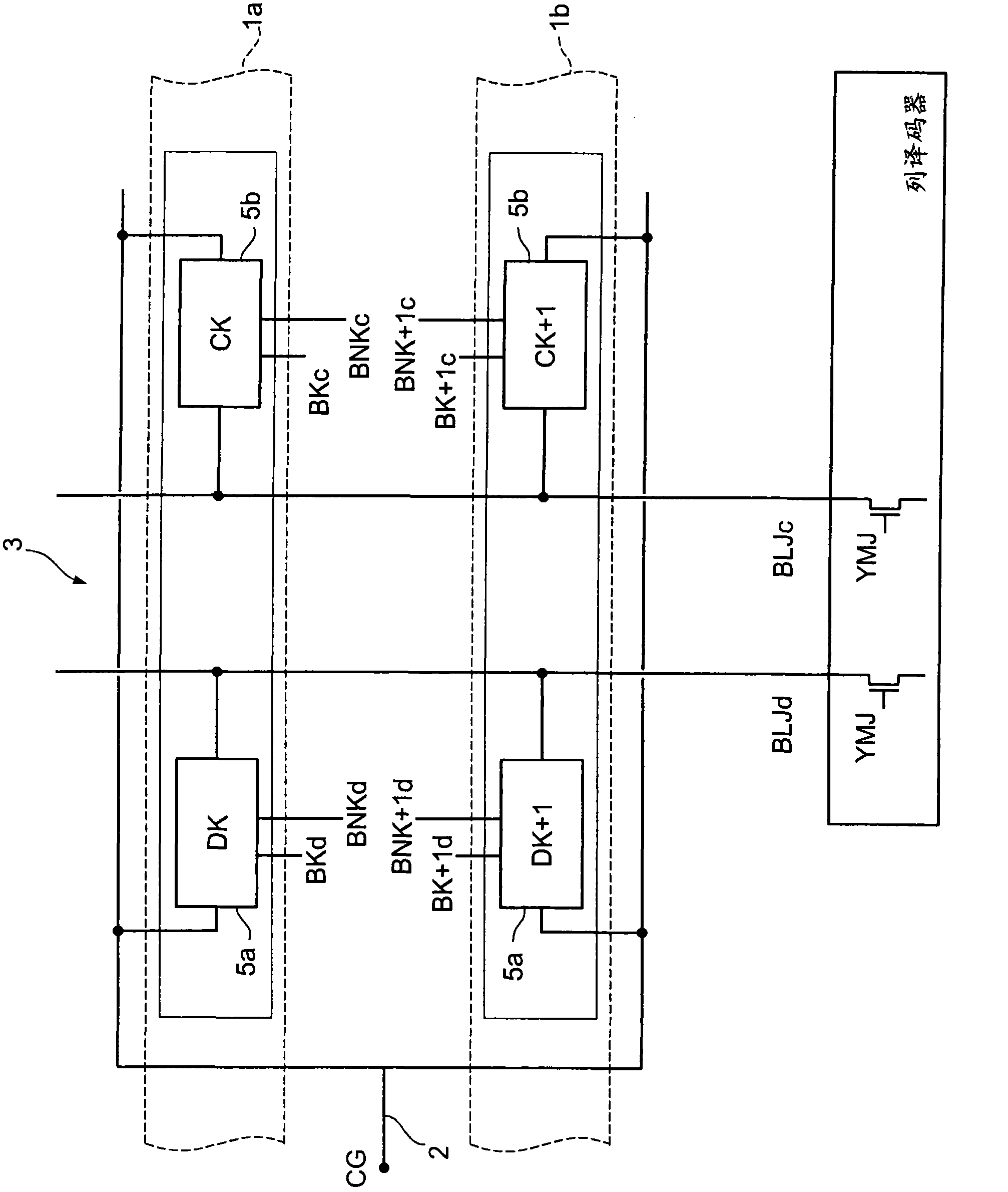
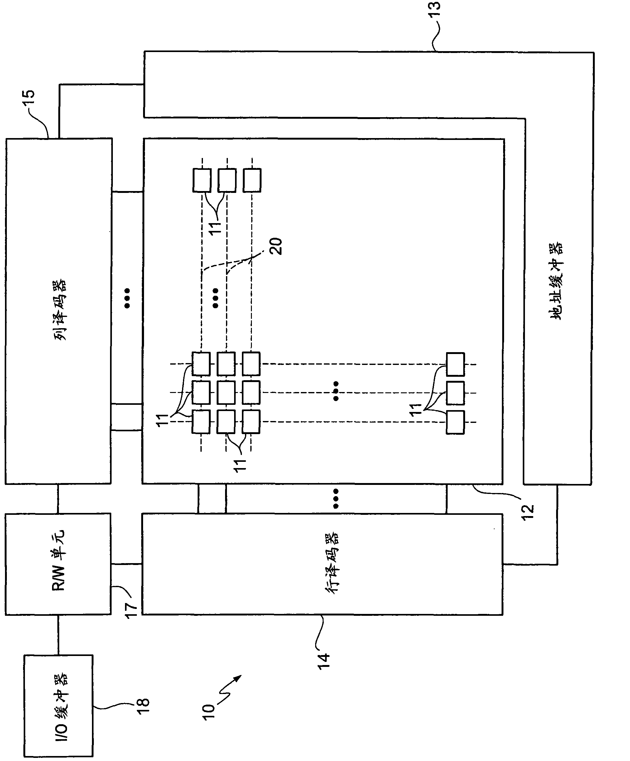
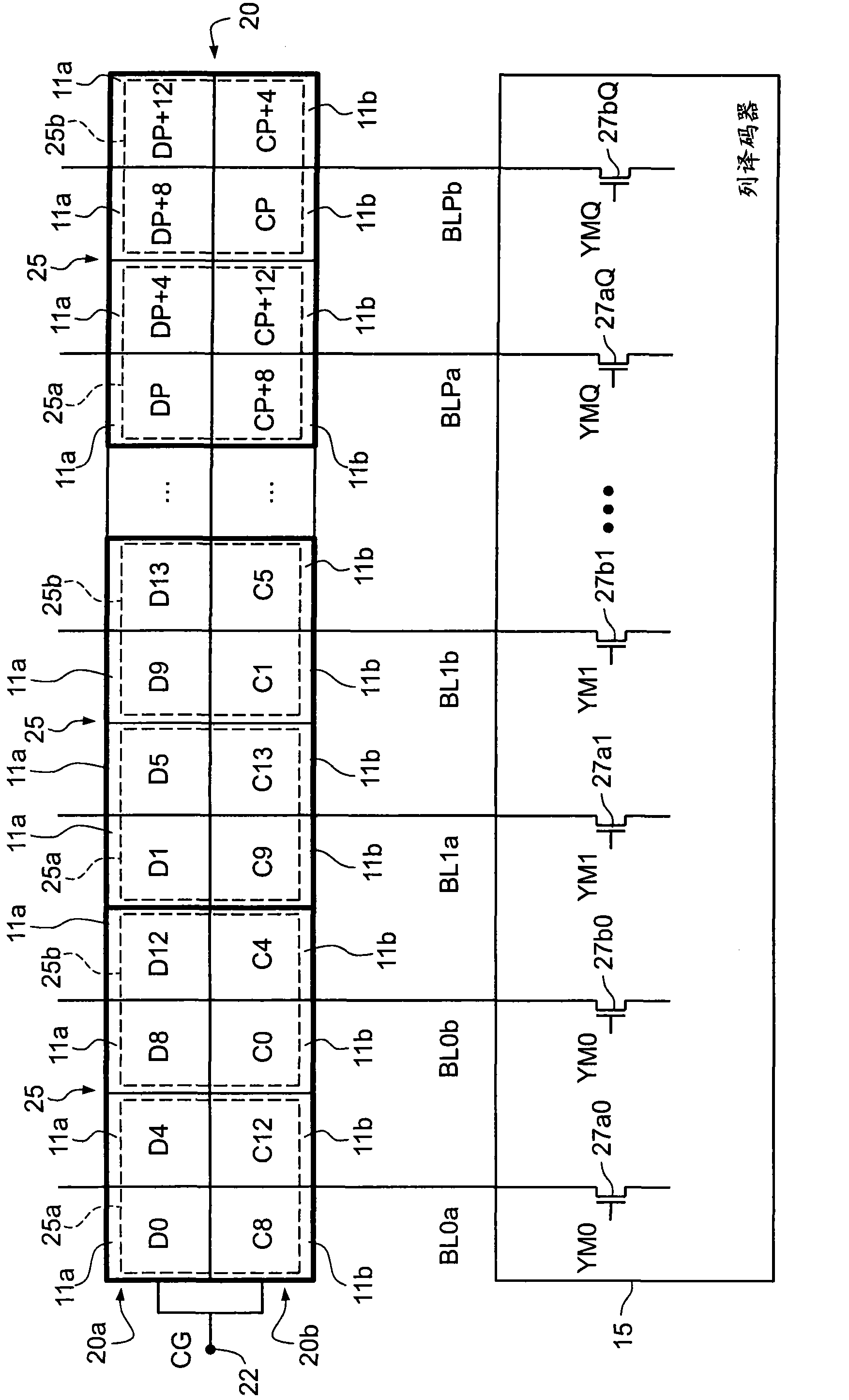
[0021] refer to figure 2 , the differential nonvolatile memory device is labeled with reference numeral 10 and includes a plurality of nonvolatile logical memory cells 11 organized in logical rows 20 and logical columns 21 to form Array 12 (eg, 128-512 rows and 512-1024 columns).

[0022] The memory device 10 further includes an address buffer 13, a row decoder 14, a column decoder 15, a read / write unit 17, and an input / output buffer 18 (hereinafter, the term "write" is used to neutrally refer to a logical memory unit 11 program and erase operations).

[0023] Address buffer 13 receives addresses of cells selected from pages of array 12 . The row and column portions of the address are provided to row decoder 14 and column decoder 15 , which select corresponding rows and columns of array 12 .

[0024] The read / write unit 17 controls the row decoder 14 and the column decoder 15, and has components required for programming, erasing and reading operations of memory cells (incl...


PUM


Abstract

An embodiment of a non-volatile memory device includes: a memory array, having a plurality of non-volatile logic memory cells arranged in at least one logic row, the logic row including a first row and a second row sharing a common control line; and a plurality of bit lines. Each logic memory cell has a direct memory cell, for storing a logic value, and a complementary memory cell, for storing a second logic value, which is complementary to the first logic value in the corresponding direct memory cell. The direct memory cell and the complementary memory cell of each logic memory cell are coupled to respective separate bit lines and are placed one in the first row and the other in the second row of the respective logic row.

Description

technical field [0001] The present invention relates to non-volatile memory devices having clustered memory cells. Background technique [0002] It is well known that several integrated electronic devices require a certain amount of non-volatile memory. Non-volatile memory may conventionally be used in a stand-alone memory board or card that is separate from the chip that integrates the control and processing functions of the device. However, in some cases it is desirable to provide the processing unit with an embedded non-volatile memory integrated in the same chip. [0003] In conventional stand-alone nonvolatile memory devices, the structure of the memory cells is not easily integrated in the CMOS fabrication process widely used to fabricate processing and control components. Especially for standard CMOS process flows, floating gate cells usually require an additional polysilicon layer. Therefore, the integration of nonvolatile memory cells in standard CMOS processes w...

Claims


Application Information

Patent Timeline
IPC IPC(8): G11C16/06
CPCG11C7/18G11C5/02G11C16/00G11C8/12G11C16/24G11C5/025G11C16/08
Inventor F·德桑蒂斯M·帕索蒂A·拉尔
Owner STMICROELECTRONICS SRL
Why Eureka
Try Eureka