Method for centering and positioning self-centering positioning chuck and semiconductor wafer

A self-centering and chucking technology, used in semiconductor/solid-state device manufacturing, electrical components, circuits, etc., can solve the problems that the positioning accuracy needs to be improved, the adaptability of the wafer diameter is not strong, and the positioning accuracy can be improved. Effect

Inactive Publication Date: 2014-02-19
THE 45TH RES INST OF CETC
View PDF4 Cites 27 Cited by
  • Summary
  • Abstract
  • Description
  • Claims
  • Application Information

AI Technical Summary

Problems solved by technology

[0005] The invention provides a self-centering positioning chuck and a centering positioning method for semiconductor wafers, which solves the problem of simultaneously performing centering and positioning based on sensor measurement of peripheral information in the prior art, strong information correlation, and adaptability to wafer diameters. The performance is not strong, and the positioning accuracy needs to be improved

Method used


Image

  • Method for centering and positioning self-centering positioning chuck and semiconductor wafer
  • Method for centering and positioning self-centering positioning chuck and semiconductor wafer
  • Method for centering and positioning self-centering positioning chuck and semiconductor wafer

Examples


Embodiment Construction

[0036] The invention relates to a self-centering positioning chuck and a centering and positioning method for semiconductor wafers. Figure 1~5 The structures and methods of the present invention are described in certain representative examples.

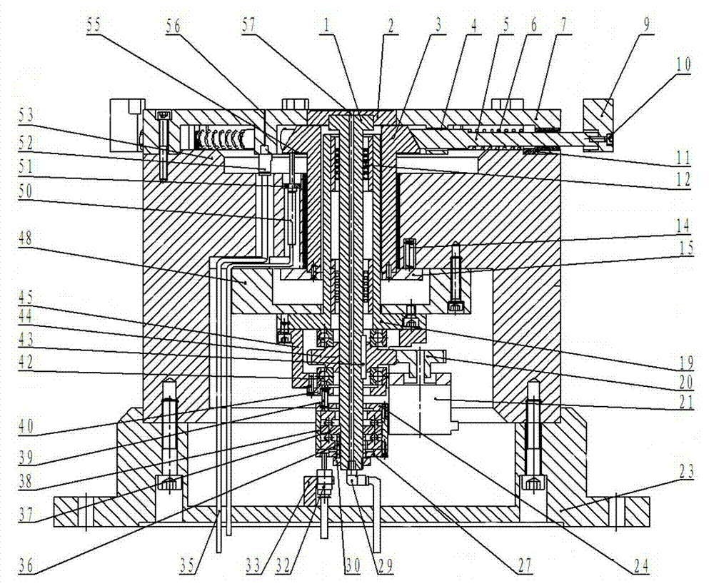
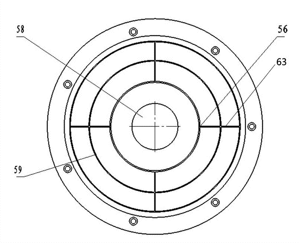
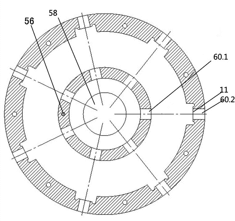
[0037] attached figure 1 The self-centering positioning chuck cuts the internal structure diagram, a self-centering positioning chuck includes a tray 7, a chuck positioning component, a central adsorption component and a chuck shell, and the chuck shell includes a base 23 and an intermediate seat The cover 53 is characterized in that: the tray 7 is a disk with a through hole 58 in the center, and two concentric inner rings 62.1 and outer rings 62.2 are fixedly connected to the lower end surface of the disk, and the inner ring 62.1 There are radial, evenly distributed inner through holes 60.1 and outer through holes 60.2 on the ring wall of the outer ring 62.2 respectively, the diameters of the inner through holes 60.1 and the outer ...


PUM


Abstract

Provided is a method for centering and positioning a self-centering positioning chuck and a semiconductor wafer. The self-centering positioning chuck comprises a tray, a positioning assembly, a center absorption assembly and a chuck shell, wherein the tray is radially provided with telescopic rods capable of freely stretching and retracting axially, and a needle air cylinder communicated with an air source acts on the telescopic rods through a taper-face shaft so that the telescopic rods can stretch; the middle sections of the telescopic rods are sleeved with springs with a pushing function, and the telescopic rods retract and clamp the wafer under the action of the springs for centering; a sucker is arranged in the center of the tray and can rise or rotate; a clamping block can clamp and release the wafer so that the wafer can be centered; a sensor measures the positioning opening in the outer edge of the wafer for positioning the wafer. The invention provides a device for self-centering and positioning of the semiconductor wafer. The device can be applied to equipment for detecting chips in the IC industry, and can be applied to equipment for processing the wafer.

Description

technical field [0001] The invention relates to a positioning device for a semiconductor wafer, in particular to a self-centering positioning chuck capable of centering and positioning the wafer and a centering and positioning method for the semiconductor wafer. Background technique [0002] In the IC industry, the diameter of wafers is increasing, and integrated circuit devices are developing towards small volume and high density. The integration level is getting higher and higher, and the requirements for testing equipment are getting higher and higher. Pollution, high intelligence and automation become research hotspots. [0003] The requirement for chip inspection equipment for large-diameter wafers is to realize automatic measurement, so the wafer needs to be precisely centered and positioned during the wafer transfer process. [0004] At present, the wafer positioning device disclosed in the prior art measures the peripheral position of the semiconductor wafer through...

Claims


Application Information

Patent Timeline
Patent Type & Authority Applications(China)
IPC IPC(8): H01L21/68H01L21/687
CPCH01L21/68H01L21/6838
Inventor 胡晓霞
Owner THE 45TH RES INST OF CETC
Why Eureka
Try Eureka