COB packaging structure of light-emitting diode

A technology of light-emitting diodes and packaging structures, applied in semiconductor/solid-state device components, semiconductor devices, electrical components, etc., can solve problems such as complex circuits, achieve high density, reduce precision requirements, and save the number of pins

Inactive Publication Date: 2014-02-19
GUANGDONG VTRON TECH CO LTD
View PDF7 Cites 17 Cited by
  • Summary
  • Abstract
  • Description
  • Claims
  • Application Information

AI Technical Summary

Problems solved by technology

However, this solution also has certain defects, and it still cannot solve the problem of complex circuits to a greater extent, as well as the problems of reducing packaging costs and improving welding efficiency.

Method used


Image

  • COB packaging structure of light-emitting diode
  • COB packaging structure of light-emitting diode
  • COB packaging structure of light-emitting diode

Examples


Embodiment 1

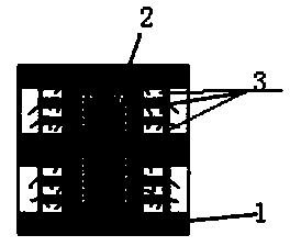
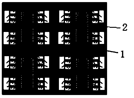
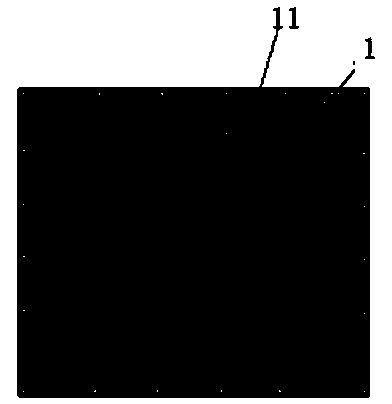
[0022] Such as Figure 1-3 As shown, a COB packaging structure of light-emitting diodes includes a substrate 1, n driver chips 2 and n light-emitting diode chip groups 3, each light-emitting diode chip group includes N light-emitting diode chips, where n and N are integers and n≥1, N≧1; n driver chips 2 and n LED chipsets 3 are packaged in a modular form on the front of the substrate 1 to form a COB display module, n driver chips 2 and n LED chipsets 3 A one-to-one connection is used to form a lamp drive coplanar device group. A fixed number of pads 11 are provided on the back of the substrate 1. Each driver chip 2 and each light-emitting diode chip group 3 are soldered to the back of the substrate 1 through wiring vias. Disk 11 communicates.

[0023] In the present invention, through the circuit design of the substrate 1, it is changed to N lamp driver coplanar devices (CIS) to form a new COB device, which saves a large number of pins, greatly reduces the difficulty of PCB d...


PUM


Abstract

The invention relates to a COB packaging structure of a light-emitting diode. The COB packaging structure comprises a substrate, n drive chips and n light-emitting diode chip sets, wherein each light-emitting diode chip set comprises N light-emitting diode chips, n and N are integers, n is larger than or equal to 1, N is larger than or equal to 1, the n drive chips and the n light-emitting diode chip sets are packaged on the front face of the substrate in a modular mode to form n sets of COB display modules, the n drive chips and the n light-emitting diode chip sets form lamp-driver co-plane devices in a one-to-one connection mode, a fixed number of bonding pads are arranged on the back face of the substrate, and all the drive chips and all the light-emitting diode chip sets are communicated with the bonding pads on the back face of the substrate in a routing and hole passing mode. The n lamp-driver co-plane devices are packaged to form a new COB device, the number of the bonding pads on the back face of the substrate is fixed and independent of the number of sets of the drive chips, and therefore a large number of pins are saved, external device cables are greatly reduced, and the higher density can be achieved compared with the density achieved through traditional packaging.

Description

technical field [0001] The present invention relates to the technical field of light emitting diode packaging, and more specifically, to a COB packaging structure of light emitting diodes. Background technique [0002] In the high-resolution display industry, the dot pitch between LED (Light Emitting Diode) chips determines the resolution of the LED display per unit area. Therefore, under the high-resolution requirement, adjacent LED pixels should be reduced The distance between them has become the key improvement direction in the industry. [0003] In the traditional way of placing the driver chip and LED on both sides of the PCB (Printed Circuit Board), in the high-density field, in order to connect each line to the pins of the driver chip on the back of the PCB, the number of layers of the PCB needs to be continuously increased. Increasing, PCB drilling aperture continues to shrink, has begun to challenge the supporting capacity of the PCB manufacturing industry, and bri...

Claims


Application Information

Patent Timeline
Patent Type & Authority Applications(China)
IPC IPC(8): H01L25/16H01L33/62H01L23/488
CPCH01L2224/48091H01L2224/48137H01L2924/00014
Inventor 董萌胡新喜孙天鹏李春辉佘星欣
Owner GUANGDONG VTRON TECH CO LTD
Why Eureka
Try Eureka