Photonic crystal three-resonant cavity athermalization biosensor

A biosensor and photonic crystal technology, applied in the field of biosensors, can solve the problems of waste of area, long distance between the reference resonant cavity and the detection resonant cavity, and the impossibility of providing valuable reference values, achieving high integration and no need for temperature control device, the effect of avoiding measurement deviation

Active Publication Date: 2014-03-05
UNITED MICROELECTRONICS CENT CO LTD
View PDF4 Cites 6 Cited by
  • Summary
  • Abstract
  • Description
  • Claims
  • Application Information

AI Technical Summary

Problems solved by technology

However, this method also has some inherent disadvantages
Due to the high integration characteristics of biosensors based on resonant cavities, a chip can integrate hundreds of sensing units. If a whole biosensing chip is equipped with only one reference resonant cavity, the distance between the reference resonant cavity and the detection resonant cavity will be too large. In actual application, if the temperature of the chip is not uniform, the reference resonator cannot provide a valuable reference value
However, if a reference resonant cavity is arranged in each sensing unit, there will be a waste of area, which is not conducive to the design and manufacture of highly integrated biosensing chips.

Method used


Image

  • Photonic crystal three-resonant cavity athermalization biosensor
  • Photonic crystal three-resonant cavity athermalization biosensor
  • Photonic crystal three-resonant cavity athermalization biosensor

Examples


Embodiment Construction

[0025] In order to make the object, technical solution and advantages of the present invention clearer, the present invention will be further described in detail below in conjunction with the accompanying drawings and embodiments. It should be understood that the specific embodiments described here are only used to explain the present invention, not to limit the present invention.

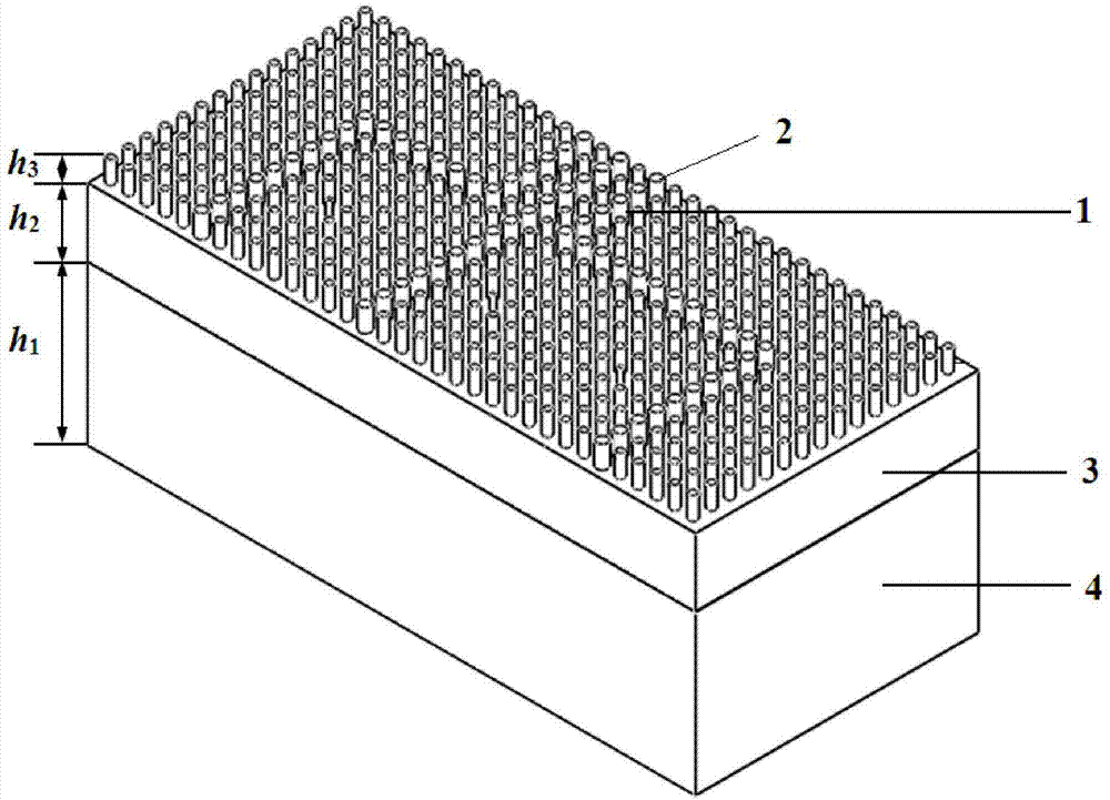
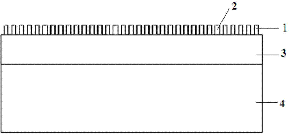
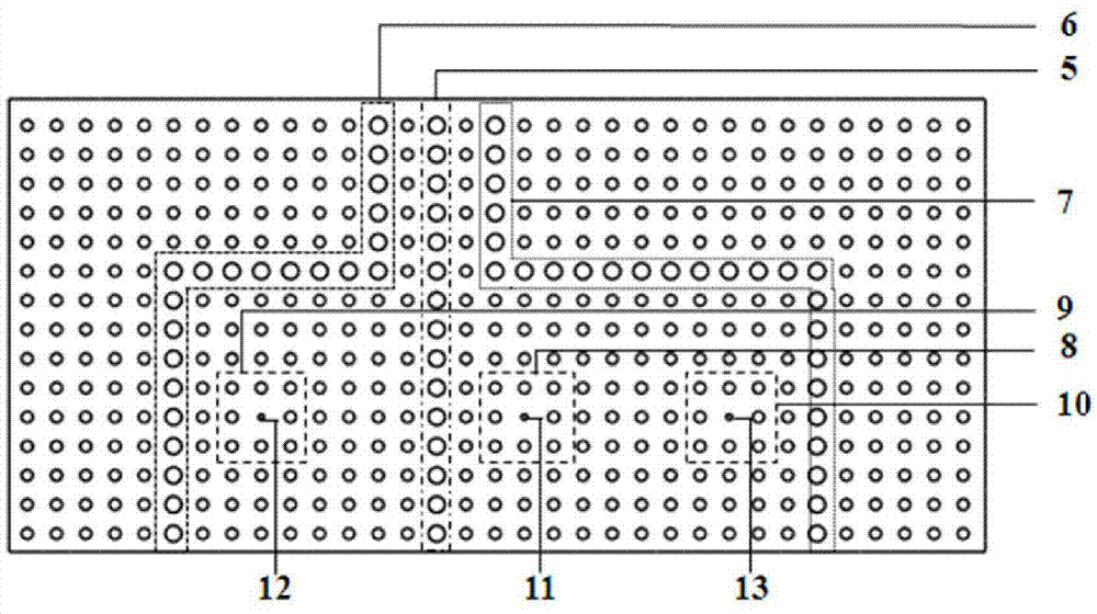
[0026] like figure 1 , 2 , 3 and 4 are schematic structural diagrams of the photonic crystal triple resonant cavity athermal biosensor provided by the preferred embodiment of the present invention. The photonic crystal three-cavity athermal biosensor includes a substrate and several first dielectric pillars 1 and several second dielectric pillars 2 arranged vertically on the substrate in a matrix. The radius of the first dielectric column 1 is r, and the radius of the second dielectric column 2 is r a , and r≠r a .

[0027]The plurality of second dielectric pillars 2 are divided into three par...


PUM

PropertyMeasurementUnit
thicknessaaaaaaaaaa
thicknessaaaaaaaaaa
depthaaaaaaaaaa

Abstract

The invention discloses a photonic crystal three-resonant cavity athermalization biosensor. The photonic crystal three-resonant cavity athermalization biosensor comprises a substrate, as well as a plurality of first dielectric cylinders and a plurality of second dielectric cylinders which are vertically arranged on the substrate in a matrix manner, wherein the radiuses of the first dielectric cylinders are r, the radiuses of the second dielectric cylinders are ra, r is not equal to ra, wherein the plurality of second dielectric cylinders are divided into three parts to form a main waveguide and two coupling waveguides respectively, the two coupling waveguides are respectively and symmetrically arranged on two sides of the main waveguide, the main waveguide is linear and is a photonic crystal straight waveguide, the two coupling waveguides are in a shape of quarter turn, the plurality of first dielectric cylinders are filled among the main waveguide and the two coupling waveguides which are mutually independent, three photonic crystal resonant cavities are arranged between the two coupling waveguides and the main waveguide, and the main waveguide and the two coupling waveguides are respectively coupled with the three photonic crystal resonant cavities.

Description

technical field [0001] The invention relates to a biological sensor, in particular to an athermalized biological sensor with a photonic crystal triple resonant cavity. Background technique [0002] Biosensors use biologically active units as biologically sensitive units and are highly selective detectors for analytes. They have important applications in environmental monitoring, biological defense, food testing, disease monitoring, and drug development. In recent years, with the development of photonic integration technology and the concept of Lab-on-a-chip (Lab-on-a-chip), biosensors based on photonic crystal resonators have the advantages of fast detection speed, high sensitivity, good real-time performance, It has become one of the research hotspots in the field of biosensing due to the advantages of no labeling, no interference from environment and power frequency. [0003] The biosensor market is huge and is on the rise every year. According to Market Research, a profe...

Claims


Application Information

Patent Timeline
Patent Type & Authority Applications(China)
IPC IPC(8): G01N21/41G02B6/122
Inventor 崔乃迪郭进冯俊波滕婕周杰
Owner UNITED MICROELECTRONICS CENT CO LTD
Why Eureka
Try Eureka