Semiconductor encapsulation electromagnetic shielding structure and manufacturing method

A technology of electromagnetic shielding structure and manufacturing method, which is applied to semiconductor devices, semiconductor/solid-state device parts, circuits, etc., can solve problems such as the treatment of radiation leakage from chips 112, and achieve low cost, low overall cost, and cost advantages obvious effect

Inactive Publication Date: 2014-03-05
NAT CENT FOR ADVANCED PACKAGING
View PDF4 Cites 10 Cited by
  • Summary
  • Abstract
  • Description
  • Claims
  • Application Information

AI Technical Summary

Problems solved by technology

The shielding case 101 takes into account the mutual interference between the shielding chi

Method used


Image

  • Semiconductor encapsulation electromagnetic shielding structure and manufacturing method
  • Semiconductor encapsulation electromagnetic shielding structure and manufacturing method
  • Semiconductor encapsulation electromagnetic shielding structure and manufacturing method

Examples


Embodiment Construction

[0029] The present invention will be further described below in conjunction with specific drawings and embodiments.

[0030] Such as Figure 5 Shown:

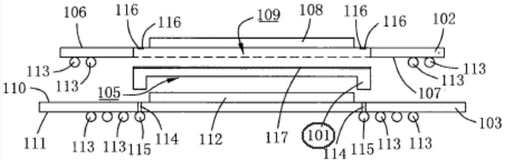
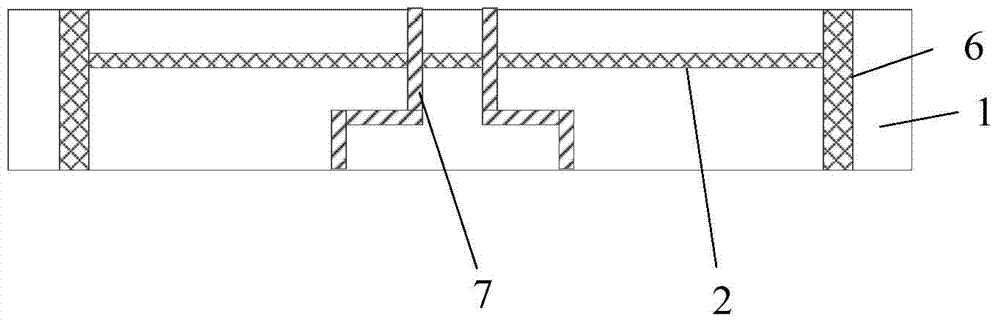
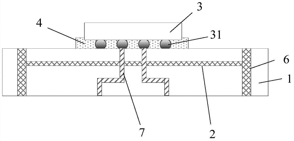
[0031] An electromagnetic shielding structure for a semiconductor package proposed by the present invention includes an organic substrate 1, the organic substrate 1 has two opposite conductor surfaces, and at least one layer of metal shielding is provided in the organic substrate 1 between the two conductor surfaces. Layer 2; wherein the conductor surface means that the surface of the organic substrate 1 is provided with a wiring layer, and does not mean that the surface of the organic substrate 1 is completely a conductive layer.

[0032] The chip 3 is mounted on a conductor surface of the organic substrate 1 , and the connection bump 31 of the chip 3 is connected to the conductor surface; the bottom of the chip 3 is filled with a chip underfill 4 .

[0033] The electromagnetic shielding cover 5 is fixed on the conductor sur...


PUM


Abstract

The invention provides a semiconductor encapsulation electromagnetic shielding structure which comprises an organic substrate. The organic substrate is provided with two opposite conductor faces, and the part, between the two conductor faces, of the organic substrate is internally provided with at least one metal shielding layer. A chip is attached to one conductor face of the organic substrate, and connecting protruding points of the chip are connected with the conductor face. An electromagnetic shielding cover is fixed on the conductor face to which the chip is attached and covers the chip completely inside the electromagnetic shielding cover. The bottom of the side wall of the electromagnetic shielding cover is electrically connected with the metal shielding layer and the other conductor face of the organic substrate through an electric flux hole penetrating through the organic substrate. The connecting protruding points, related to a signal and a power source, of the chip are electrically connected with the other conductor face of the organic substrate through a signal and a power source channel which penetrates through the organic substrate and is insulated from the metal shielding layer. According to the semiconductor encapsulation electromagnetic shielding structure, both faces of the chip can be provided with electromagnetic shielding structure bodies, a better electromagnetic shielding effect can be obtained, and the advantage in cost is obvious when the semiconductor encapsulation electromagnetic shielding structure is manufactured on a large scale.

Description

technical field [0001] The invention relates to a package structure, in particular to a semiconductor package electromagnetic shielding structure. Background technique [0002] At present, with the trend of multi-function and miniaturization of electronic products, high-density microelectronic assembly technology has gradually become the mainstream in the new generation of electronic products, especially in hand-held portable products. The sudden increase in micro-assembly density and integration has put forward higher requirements for electromagnetic shielding of devices with strong electromagnetic radiation in a limited space, and the process difficulty has increased. [0003] figure 1 It is an existing electromagnetic shielding solution, which is mainly to install an electromagnetic shielding cover on the semiconductor packaging structure to shield the electromagnetic interference between chips. However, the leakage of electromagnetic radiation from the bottom of the de...

Claims


Application Information

Patent Timeline
IPC IPC(8): H01L23/552H01L23/12
CPCH01L2224/16227H01L2224/16235H01L2224/32225H01L2224/73204H01L2924/15311H01L2924/16251H01L2924/3025H01L2224/16225H01L2924/00
Inventor 王宏杰徐健孙鹏
Owner NAT CENT FOR ADVANCED PACKAGING
Why Eureka
Try Eureka