High-frequency module and method for inspecting high-frequency module

A high-frequency module and high-frequency circuit technology, used in RF circuit testing, instruments, semiconductor/solid-state device testing/measurement, etc., can solve problems such as soaring manufacturing costs and high-frequency module characteristics that do not meet specifications

Inactive Publication Date: 2014-03-05
PANASONIC CORP
View PDF7 Cites 2 Cited by
  • Summary
  • Abstract
  • Description
  • Claims
  • Application Information

AI Technical Summary

Problems solved by technology

[0002] In high-frequency modules, when flip-chip assembly is performed, the characteristics of the circuit chip change due to the height of the bumps at the time of assembly, and the failure of high-frequency module characteristics that do not meet the specifications increases.
However, the evaluation of such a module requires the use of expensive equipment, so there is a concern that the manufacturing cost will skyrocket

Method used


Image

  • High-frequency module and method for inspecting high-frequency module
  • High-frequency module and method for inspecting high-frequency module
  • High-frequency module and method for inspecting high-frequency module

Examples


Embodiment approach 1

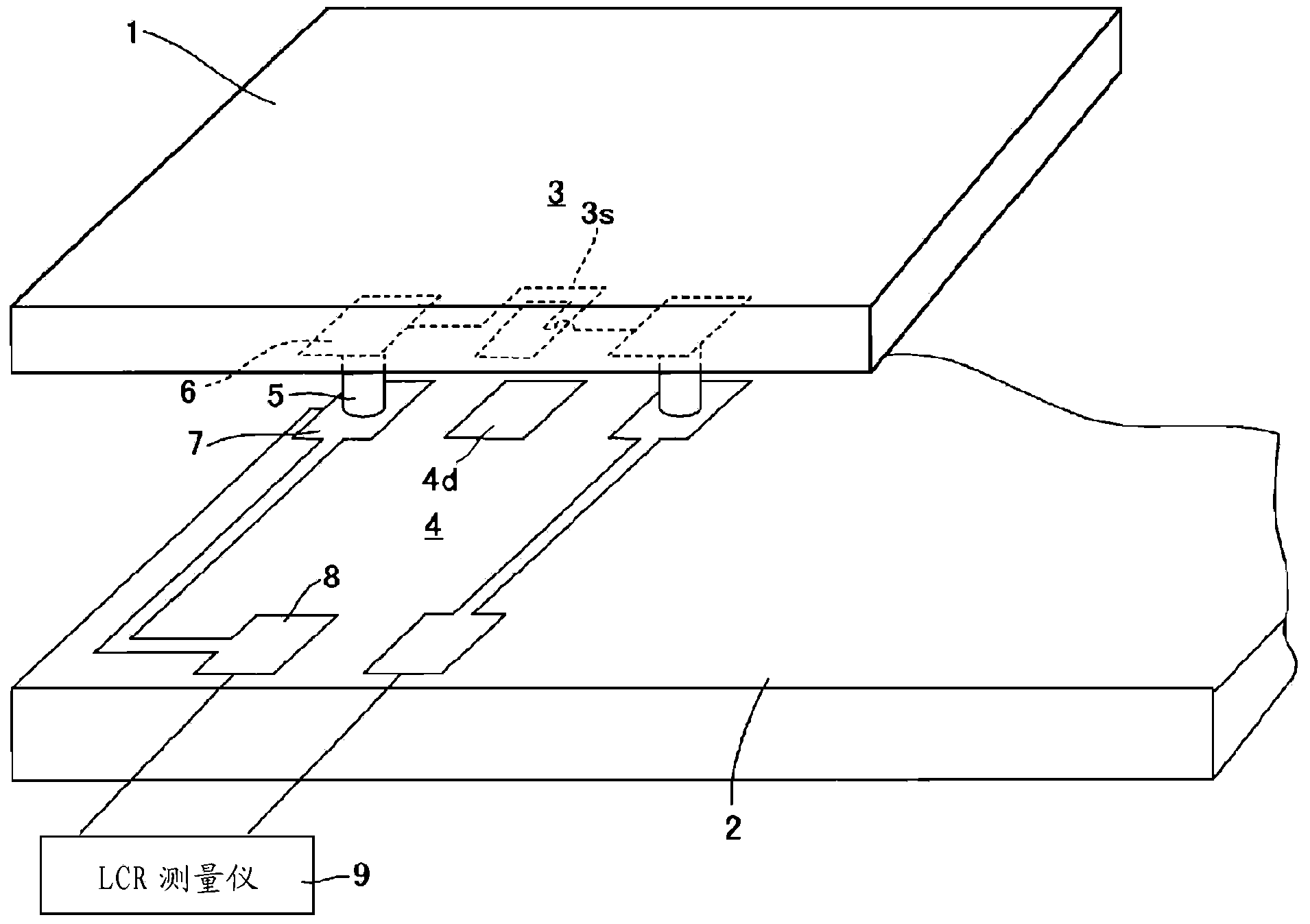
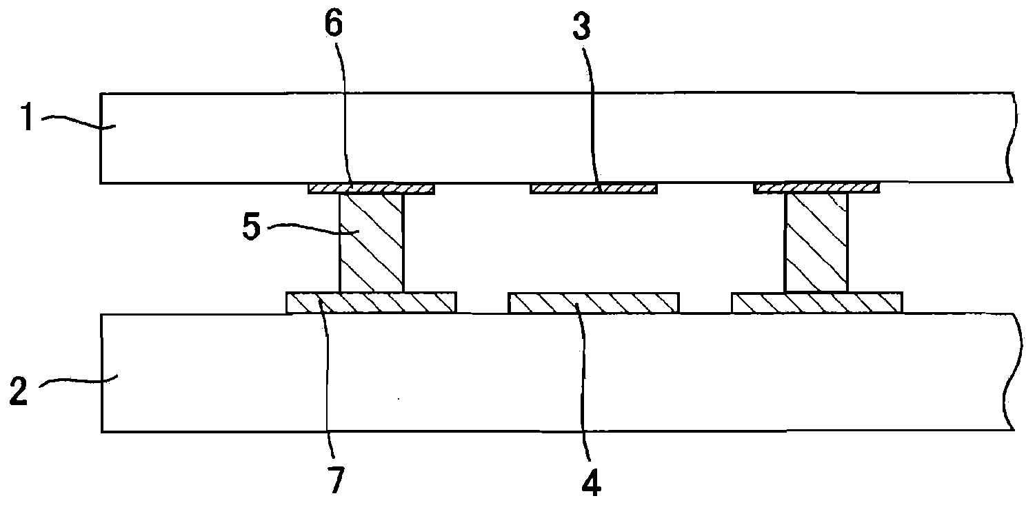
[0067] figure 1 It is an explanatory diagram (perspective view) showing the structure of the high-frequency module according to Embodiment 1 of the present invention, figure 2 is a cross-sectional view. In this embodiment, an example in which a spiral inductor is used as a circuit element for measurement will be described.

[0068]The high-frequency module includes a high-frequency circuit chip 1, a wiring substrate 2 as a module substrate on which the high-frequency circuit chip 1 is assembled, a first circuit 3 formed on the high-frequency circuit chip 1, a second circuit 4 formed on the wiring substrate 2, Bumps 5 connecting electrodes of the high-frequency circuit chip 1 and the wiring board 2 , input / output terminals (electrodes) 6 on the high-frequency circuit chip 1 , and connection pads (electrodes) 7 of the wiring board 2 .

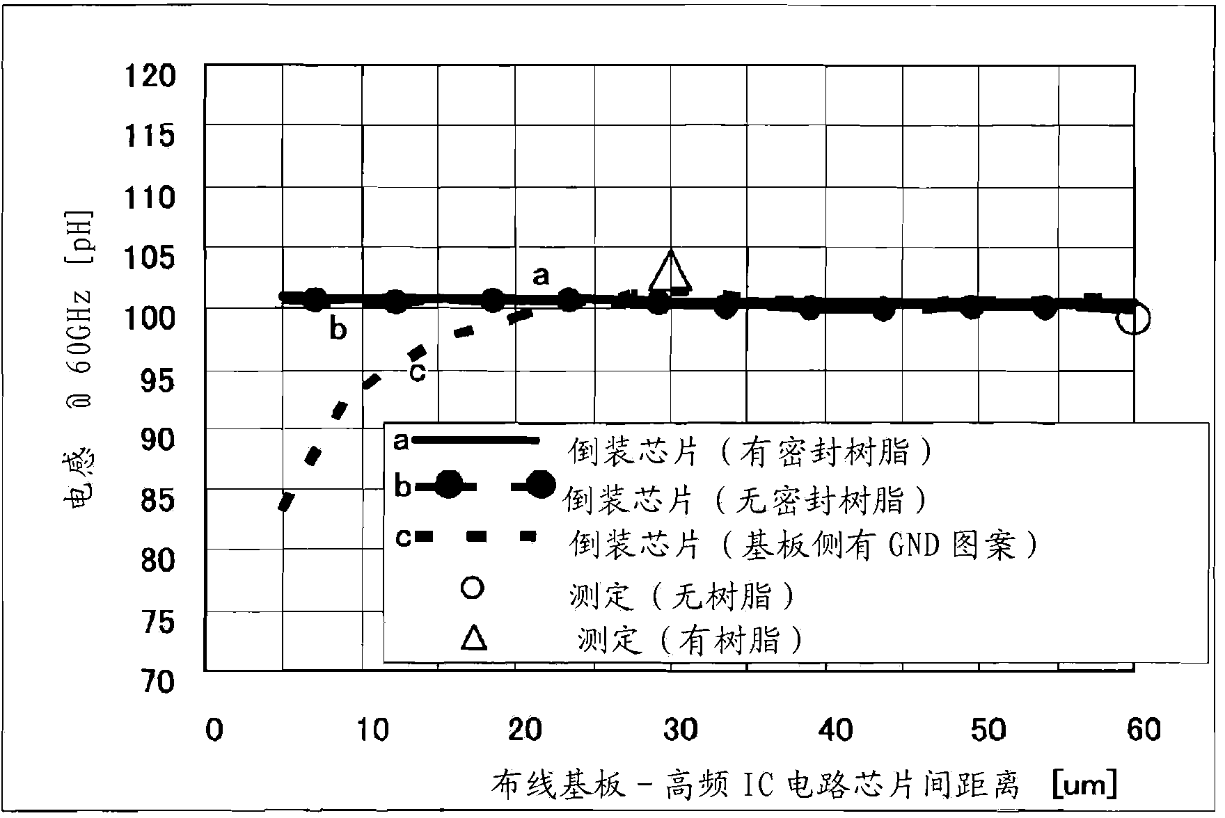
[0069] For example, the first circuit 3 is configured using a spiral inductor 3s, and the second circuit 4 is configured using a detection c...

Embodiment approach 2

[0088] Next, Embodiment 2 of the present invention will be described.

[0089] In the high-frequency module of Embodiment 1, such as Figure 4 As shown in the middle perspective view, the spiral inductor 3s is formed on the high-frequency circuit chip 1, and the detection conductor 4d is formed on the wiring board 2 as the second circuit 4. However, in the high-frequency module according to Embodiment 2, the detection conductor 3d is disposed on the high-frequency circuit chip 1 , and the spiral inductor 4s is disposed on the wiring board 2 .

[0090] Others are the same as those in Embodiment 1, so explanations are omitted here.

[0091] In this embodiment, as in the high-frequency module of Embodiment 1, the inductance caused by the change in the distance between the spiral inductor 3s and the detection conductor 4d is detected by measuring the change in inductance between the connection pads 7 The change of the distance between the input-output terminal 6 and the connecti...

Embodiment approach 3

[0096] Next, Embodiment 3 of the present invention will be described. In addition, in Embodiments 1 and 2, the conductor for detection is formed on the high-frequency circuit chip 1 or the wiring board 2, but as Figure 5 As shown, a detachable outer conductor 4o may also be used.

[0097] On the wiring board 2, the outer conductor mounting part 2o is formed in advance, and the outer conductor 4o is arranged on the outer conductor mounting part 2o, and the distance between the high-frequency circuit chip 1 and the wiring board is measured in the same way as in Embodiments 1 and 2, and bumps are detected. high. The other parts are the same as those of the high-frequency module according to Embodiment 1, so explanations are omitted here.

[0098] That is, the high-frequency module according to Embodiment 1 includes: a high-frequency circuit chip 1 having input and output terminals 6; The wiring substrate 2.

[0099] Furthermore, the first circuit 3 serving as a wiring portio...


PUM


Abstract

A high-frequency module is equipped with: a high-frequency circuit chip; a wiring substrate which includes connection pads for connecting input / output terminals of the high-frequency circuit chip; a spiral inductor which is connected between two terminals connected to the connection pads; and a ground potential detection conductor which is provided at a position opposite the spiral inductor. The spiral inductor is provided in either the high-frequency circuit chip or the wiring substrate, the detection conductor is provided in the other, and inductance between the connection pads is measured.

Description

technical field [0001] The invention relates to a high-frequency module and a method for inspecting the high-frequency module, in particular to a high-frequency module in which a high-frequency circuit chip is assembled in a substrate. Background technique [0002] In high-frequency modules, when flip-chip assembly is performed, the characteristics of the circuit chip change due to the height of the bumps at the time of assembly, and the number of defective high-frequency module characteristics that do not meet the specifications increases. However, the evaluation of such a module requires the use of expensive equipment, so there is a concern that the manufacturing cost will skyrocket. Therefore, there is a need for a technique capable of screening assembly failures without using expensive equipment. [0003] Therefore, the technology described in Patent Document 1 is known as a prior art of a method of measuring the assembled state of a high-frequency circuit (IC) chip. l...

Claims


Application Information

Patent Timeline
Patent Type & Authority Applications(China)
IPC IPC(8): H01L21/60G01R31/02G01R31/28
CPCH01L23/645H01L2224/81908G01R31/2822H01L24/13H01L22/14G01R31/2884H01L2224/81121G01R31/046G01R31/2601H01L23/66H01L2224/16238H01L24/16H01L24/81H01L22/34H01L2224/13005G01R31/70H01L2924/206
Inventor 藤田卓盐崎亮佑
Owner PANASONIC CORP
Why Eureka
Try Eureka