Semiconductor packaging line bonding equipment organization method based on processing task capability matching

A semiconductor and packaging wire technology, which is applied in the field of semiconductor packaging wire bonding equipment grouping, can solve the problems that equipment grouping cannot achieve dynamic matching, and can not be well matched to process LOT.

Active Publication Date: 2014-03-12
SHENYANG JIANZHU UNIVERSITY
View PDF3 Cites 2 Cited by
  • Summary
  • Abstract
  • Description
  • Claims
  • Application Information

AI Technical Summary

Problems solved by technology

[0004] The current actual semiconductor packaging online bonding equipment adopts a fixed grouping method based on the equipment sub-type, that is, once the equipment group is determined, the equipment group contains fixed equipment, resulting in the equipment group's processing capacity for the determined type of LOT is also fixed. The capacity provided by the equipment in this grouping method cannot well match the capacity required for processing LOT, and the equipment grouping cannot achieve dynamic matching with the processing tasks.

Method used


Image

  • Semiconductor packaging line bonding equipment organization method based on processing task capability matching
  • Semiconductor packaging line bonding equipment organization method based on processing task capability matching
  • Semiconductor packaging line bonding equipment organization method based on processing task capability matching

Examples


Embodiment Construction

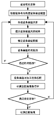
[0154] The present invention will be described in further detail below with reference to the drawings of the present invention and specific embodiments, but the protection scope of the present invention is not limited by the specific embodiments, and the claims shall prevail. In addition, on the premise of not violating the scheme of the present invention, any modification or change made to the present invention that can be easily realized by those skilled in the art will fall within the scope of the claims of the present invention.

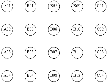
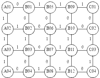
[0155] to attach figure 2 As an example, suppose there are three types of equipment A, B, and C, and the equipment names are A01 to A04, B01 to B12, and C01 to C04. The equipment is arranged in 4 rows and 5 columns, n=4, m=5, and the current batch The types of products to be processed are a and b. In the corresponding relationship between processed products and equipment models, type a products can be processed on type A equipment and type B eq...


PUM


Abstract

The invention relates to a semiconductor packaging line bonding equipment organization method based on processing task capability matching, which belongs to the technical field of semiconductor production processes. The semiconductor packaging line bonding equipment organization method is characterized in that the semiconductor packaging line bonding equipment organization method includes the following steps: bonding process equipment is abstracted into a multi-row and multi-column equipment point array; the equipment organization relations between the points in the rows and the columns are represented by '0' and '1'; an organization relation matrix and an equipment organization matrix are established; organization relations are corrected, and incomplete relation information is supplemented; equipment organization closed position relation constraint check and equipment type and processed product type matching constraint check are carried out; according to the capacities provided by equipment organizations and the capacity required by a processing task, an equipment organization is matched with the processing task; according to a matching result of the processing task and the equipment organization, punishment and a function are established, and the matching result is quantified. The semiconductor packaging line bonding equipment organization method can correspondingly organize bonding equipment according to the capacities required by processing tasks, thus meeting the requirement for the dynamic matching relation between production operations and equipment resources.

Description

technical field [0001] The invention relates to a grouping method of semiconductor packaging wire bonding equipment based on processing task capability matching, and belongs to the technical field of semiconductor production technology. Background technique [0002] The semiconductor packaging and testing process includes dicing, chip loading, bonding, plastic packaging, deflashing, electroplating, printing, rib cutting, molding, appearance inspection, finished product testing, packaging and shipping, etc. in sequence. The transformation of the processing task form is mainly controlled by the production tempo, and the production tempo control requires more process equipment for long processing time and less process equipment for short processing time, so as to ensure the continuity of production. The bonding process on the semiconductor packaging line requires the longest processing time, the largest number of equipment, and large differences in the production capacity of ea...

Claims


Application Information

Patent Timeline
Patent Type & Authority Applications(China)
IPC IPC(8): G06Q10/06G06Q50/04
CPCY02P90/30
Inventor 韩忠华曹阳林硕高恩阳孙海义
Owner SHENYANG JIANZHU UNIVERSITY
Why Eureka
Try Eureka