
Boost Converter Circuit

A technology of boost conversion circuit and boost module, which is applied in the direction of output power conversion devices, electrical components, and adjustment of electrical variables, etc., which can solve the problems of limited space and unfavorable thinning of electronic devices.

Active Publication Date: 2016-04-20
ASUSTEK COMPUTER INC
View PDF4 Cites 0 Cited by
  • Summary
  • Abstract
  • Description
  • Claims
  • Application Information

AI Technical Summary

Problems solved by technology

[0003] However, as electronic products continue to be thinner and thinner, the internal space is more limited. The volume and height of the commonly used boost converter inductor will increase with the increase of the inductance value. When the boost converter needs a larger When the output current is higher, the height required for the inductor will increase, which is not conducive to the thinning of electronic devices

Method used


Image

  • Boost Converter Circuit
  • Boost Converter Circuit
  • Boost Converter Circuit

Examples


Embodiment Construction

[0014] The boost conversion circuit according to a preferred embodiment of the present invention will be described below with reference to related drawings, wherein the same components will be described with the same reference symbols.

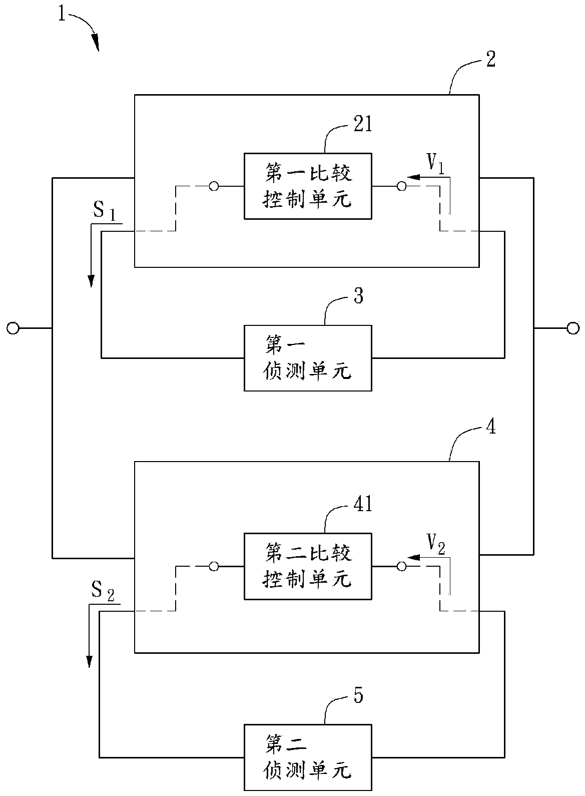
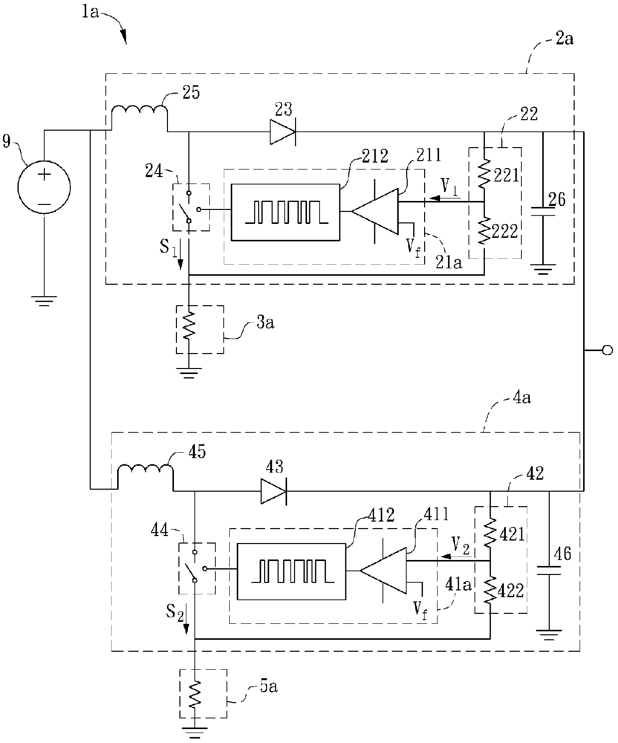
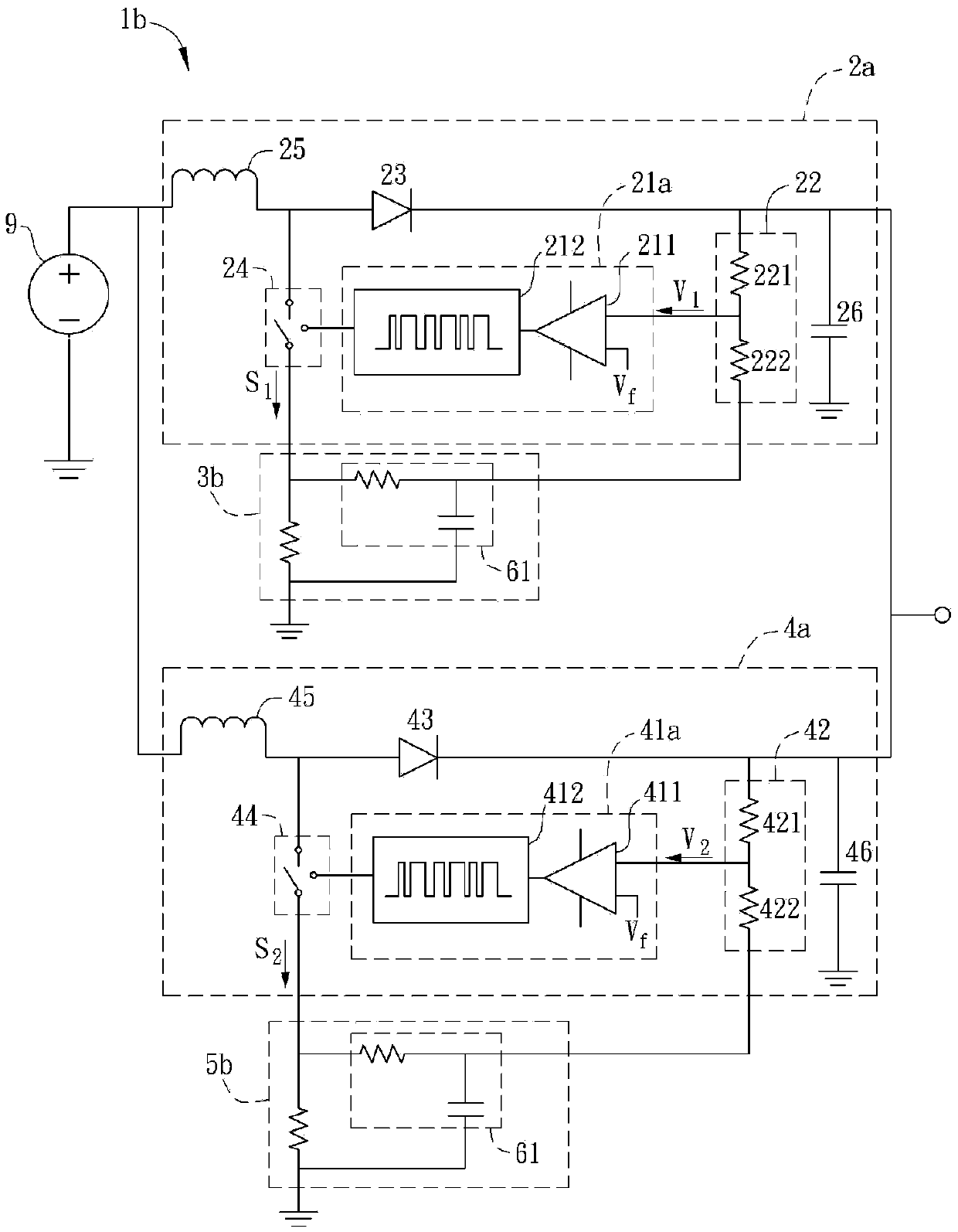
[0015] Please refer to figure 1 As shown, it is a block diagram of the boost conversion circuit of the present invention. The boost conversion circuit 1 includes a first boost module 2 , a first detection unit 3 , a second boost module 4 and a second detection unit 5 . Wherein, the first boost module 2 has a first comparison control unit 21 , the second boost module 4 has a second comparison control unit 41 , and the first boost module 2 and the second boost module 4 are connected in parallel.

[0016] The first detection unit 3 is coupled to the first boost module 2 , and the first detection unit 3 adjusts the first input signal V1 of the first comparison control unit 21 according to the first signal S1 of the first boost module 2 . The sec...


PUM


Abstract

A boost conversion circuit includes a first boost module, a first detection unit, a second boost module and a second detection unit. The first boost module has a first comparison control unit. The first detection unit is coupled to the first boost module, and the first detection unit adjusts a first input signal of the first comparison control unit according to a first signal of the first boost module. The second boost module is connected in parallel with the first boost module and has a second comparison control unit. The second detection unit is coupled to the second boost module, and the second detection unit adjusts a second input signal of the second comparison control unit according to a second signal of the second boost module. Through the cooperation of the first detection unit and the second detection unit, after the first boost module and the second boost module are connected in parallel, a larger current output can be obtained without increasing the inductance value of the inductor advantages, thereby reducing the thickness requirement of the electronic device provided with the boost conversion circuit.

Description

technical field [0001] A boost conversion circuit, especially a boost conversion circuit for a boost converter. Background technique [0002] Boost converters (boost converters) are commonly used in various electronic products to increase the input voltage to the operating voltage required by the electronic products so that the electronic products can operate normally. [0003] However, with the continuous development of electronic products in the direction of thinner and thinner, the internal space is more limited. The volume and height of the commonly used boost converter inductor will increase with the increase of the inductance value. When the boost converter needs a larger When the output current is higher, the required height of the inductor will increase, which is not conducive to the thinning of the electronic device. Contents of the invention [0004] The present invention provides a boost conversion circuit, including a first boost module, a first detection unit...

Claims


Application Information

Patent Timeline
Patent Type & Authority Patents(China)
IPC IPC(8): H02M3/10
CPCG05F1/62H02M3/1584
Inventor 蔡明廷洪祥睿许志琬涂维辰
Owner ASUSTEK COMPUTER INC
Learn More