Electronic device printing device

An electronic printing and printing device technology, applied in the direction of electric solid devices, printing, printing machines, etc., can solve the problems of high pollution treatment cost, high material consumption, complex manufacturing procedures, etc., and achieve low material ineffective loss and low environmental requirements. , the effect of reducing complexity and cost

Active Publication Date: 2014-03-26
TECHNICAL INST OF PHYSICS & CHEMISTRY - CHINESE ACAD OF SCI
View PDF11 Cites 10 Cited by
  • Summary
  • Abstract
  • Description
  • Claims
  • Application Information

AI Technical Summary

Problems solved by technology

[0007] The purpose of the present invention is to provide a device that can directly print electronic devices to solve the problems of complicated manufacturing procedures, large material consumption and high cost of pollution treatment in the existing electronic devices

Method used


Image

  • Electronic device printing device
  • Electronic device printing device
  • Electronic device printing device

Examples


Embodiment Construction

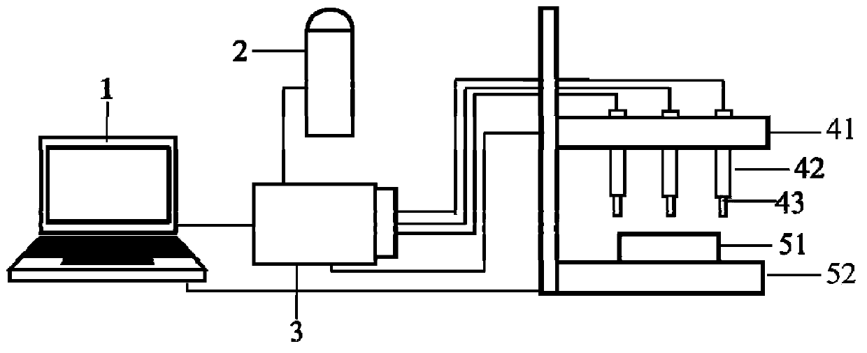
[0037] The invention provides an electronic device printing device. The printing device includes a controller, an ink cartridge array mechanism, and a substrate carrier mechanism, wherein:

[0038] The controller is used to control the ink cartridge array mechanism and the substrate carrying mechanism;

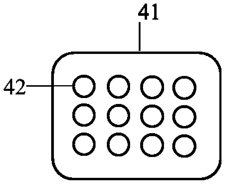
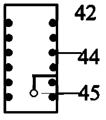
[0039] The ink cartridge array mechanism is used to provide electronic printing ink, and use the electronic printing ink to perform electronic printing;

[0040] The substrate carrying mechanism is used for carrying the electronic device substrate.

[0041] The above-mentioned electronic device substrate can be fixed on the substrate carrying mechanism by means of adhesive glue, lock buckle or negative pressure; the substrate can be selected from plastic, rubber, silicon, glass, silk fabric, polydimethylsiloxane (PDMS) , at least one of ceramics and paper.

[0042] Optionally, the device further includes a computer connected to the controller, the computer is used to genera...


PUM


Abstract

The invention provides a device which can manufacture an electronic device in a directly-printed mode. An electronic device printing device comprises a controller, an ink box array mechanism and a substrate carrying mechanism, wherein the controller is used for controlling the ink box array mechanism and the substrate carrying mechanism, the ink box array mechanism is used for providing electronic printing ink and conducting electronic printing with the electronic printing ink, and the substrate carrying mechanism is used for carrying a substrate of the electronic device. The requirements of the electronic device printing device for the environment are not high, the complexity of electronic device manufacturing process is obviously reduced, material consumption and material pollution are reduced, and the manufacturing efficiency is improved.

Description

technical field [0001] The invention relates to the technical field of electronic device manufacturing, in particular to a device capable of directly printing electronic devices. Background technique [0002] Electronic devices are generally composed of conductors, semiconductors, and insulating materials, and are widely used in a large number of research and industrial technology fields. The design and manufacture of electronic devices has always been the core of research in the field of electronics industry. So far, the processing of electronic devices has been carried out with very complicated manufacturing processes, the procedures are quite complicated, and the energy consumption is high, the pollution is serious, and the cleaning treatment costs are high. The reason is that the conductive, semi-conductive and insulating parts of electronic devices are usually deposited by high temperature or by means of chemical reaction process, which requires relatively high process...

Claims


Application Information

Patent Timeline
IPC IPC(8): B41F17/00H05K3/12H01L51/00
Inventor 刘静何志祝
Owner TECHNICAL INST OF PHYSICS & CHEMISTRY - CHINESE ACAD OF SCI
Why Eureka
Try Eureka