Array substrate, array substrate manufacturing method and display device

An array substrate and substrate technology, which is applied in the manufacture of electric solid-state devices, semiconductor devices, semiconductor/solid-state devices, etc., can solve the problems of unfavorable wide-screen display, large overlapping area of ​​common electrodes and pixel electrodes, etc., to reduce the overlapping area, The effect of saving space

Inactive Publication Date: 2014-03-26
BEIJING BOE OPTOELECTRONCIS TECH CO LTD
View PDF5 Cites 11 Cited by
  • Summary
  • Abstract
  • Description
  • Claims
  • Application Information

AI Technical Summary

Problems solved by technology

[0005] To sum up, although the current array substrate adopts a double-gate structure, the overlapping area of ​​the common electrode and the pixel electrode is too large, and the common electrode line is arranged horizontally, which is not conducive to wide-screen display.

Method used


Image

  • Array substrate, array substrate manufacturing method and display device
  • Array substrate, array substrate manufacturing method and display device
  • Array substrate, array substrate manufacturing method and display device

Examples


Embodiment Construction

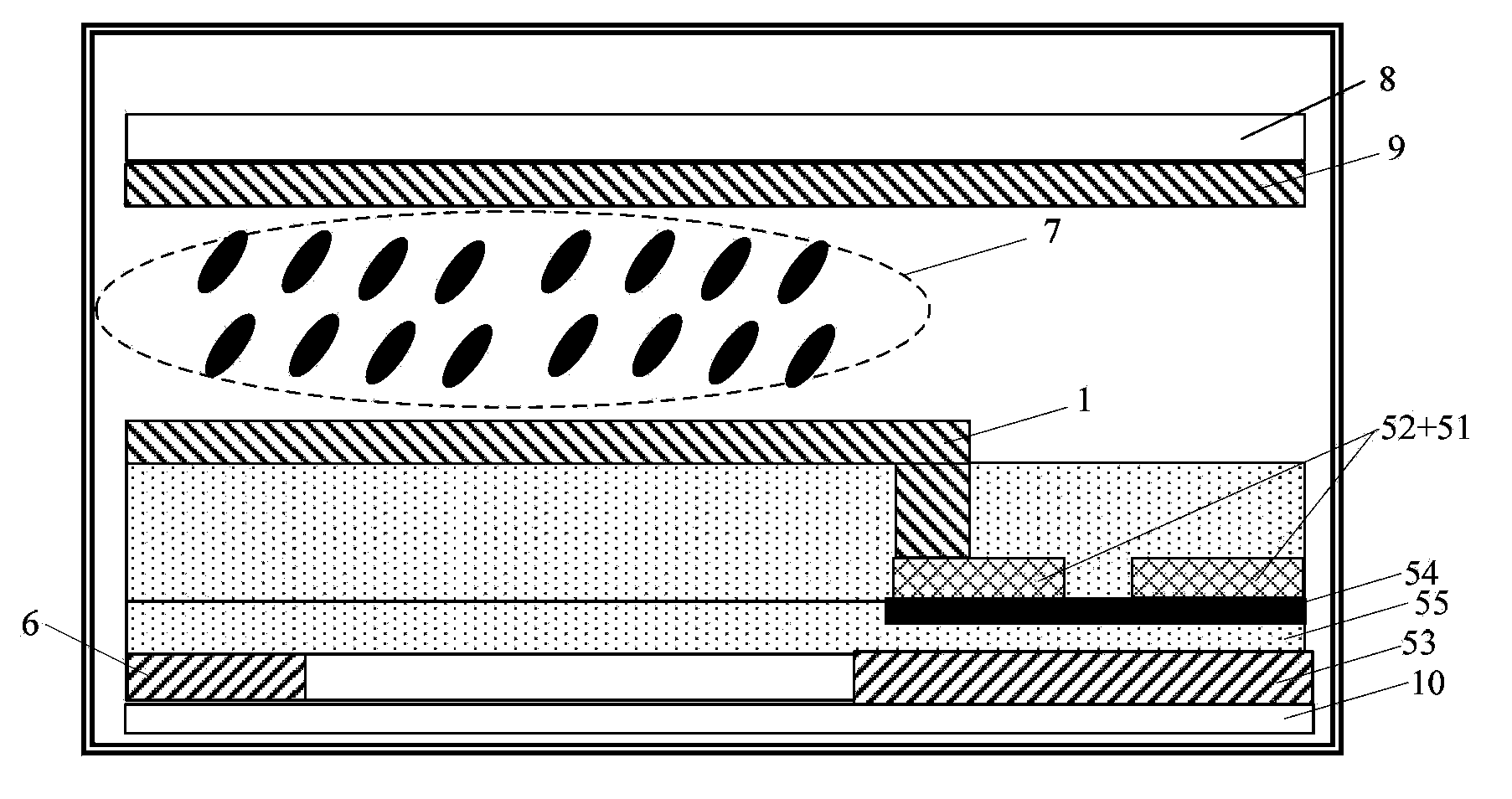
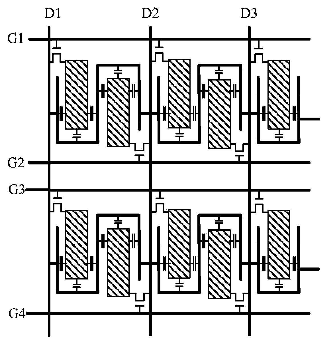
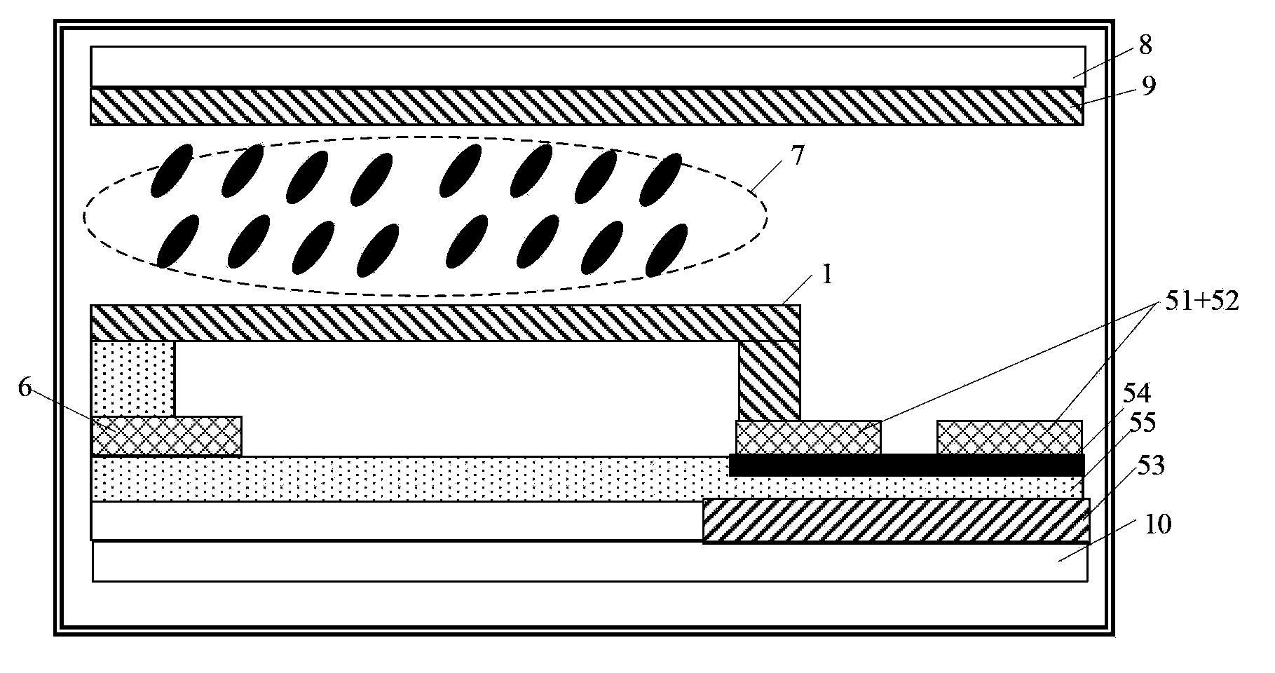
[0028] At present, the double gate structure is more and more commonly used in array substrates. The array substrate of the present invention is also based on a double-gate structure, including a substrate on which pixel regions arranged in a matrix are formed, and first pixel electrodes and first thin film transistors located in odd columns are formed in each pixel region, and first pixel electrodes located in even columns are formed. The second pixel electrode and the second thin film transistor, the drain of the first thin film transistor is connected to the first pixel electrode, the drain of the second thin film transistor is connected to the second pixel electrode, and a first gate line is formed in each pixel area and the second gate line, the first gate line is connected to the gate of the second thin film transistor, the second gate line is connected to the gate of the first thin film transistor, a data line is formed in each pixel area, and the data line is connected ...


PUM


Abstract

The invention discloses an array substrate. The array substrate comprises substrate bodies. At least one common electrode wire is formed in each pixel region of the substrate bodies. The common electrode wires are longitudinally arranged and are parallel to data lines. The invention further discloses an array substrate manufacturing method and a display device. The common electrode wires are arranged longitudinally and are parallel to the data lines. Through the adoption of the array substrate, the array substrate manufacturing method and the display device, overlapping areas can be reduced, the area is saved, and consequently widescreen display can be achieved.

Description

technical field [0001] The present invention relates to the field of display technology, in particular to an array substrate, a manufacturing method thereof, and a display device. Background technique [0002] Thin-film-transistor liquid crystal displays (TFT-LCDs), which feature small size, low power consumption, no radiation, and relatively low manufacturing costs, dominate the current flat-panel display market. [0003] For the pixel structure of the existing array substrate, the pixel is formed by interlacing data signal lines and gate signal lines, and the pixel includes a pixel electrode (pixel) and a thin film transistor (TFT) as a switch, wherein the gate of the TFT is connected to the gate pole signal line, the source is connected to the data signal line, and the drain is connected to the pixel electrode. A storage capacitor Cst is formed between the common electrode (Vcom) and the pixel electrode. [0004] Such as figure 1 as shown, figure 1 Shown is a schemati...

Claims


Application Information

Patent Timeline
Patent Type & Authority Applications(China)
IPC IPC(8): G02F1/1362G02F1/1368H01L21/77
CPCG02F1/136213G02F1/136286G02F2201/121H01L29/78669H01L29/78678H01L27/1214G02F1/133G02F1/1343G02F1/136
Inventor 黎蔚
Owner BEIJING BOE OPTOELECTRONCIS TECH CO LTD
Why Eureka
Try Eureka