Wafer reaction chamber cleaning device

A technology for reaction chambers and wafers, applied in the direction of cleaning hollow objects, cleaning methods and appliances, electrical components, etc., can solve the problems of increasing equipment costs, prolonging working hours, etc., to reduce economic losses, improve process progress, and reduce scrapping rate effect

Inactive Publication Date: 2014-03-26
SHANGHAI INTEGRATED CIRCUIT RES & DEV CENT
View PDF5 Cites 5 Cited by
  • Summary
  • Abstract
  • Description
  • Claims
  • Application Information

AI Technical Summary

Problems solved by technology

Since opening the chamber for cleaning has destroyed the vacuum environment in the chamber, it is necessary to re-adjust the machine to make the environment in the chamber meet the process requirements, which increases equipment costs and prolongs working hours.

Method used


Image

  • Wafer reaction chamber cleaning device
  • Wafer reaction chamber cleaning device
  • Wafer reaction chamber cleaning device

Examples


Embodiment Construction

[0026] Some typical embodiments embodying the features and advantages of the present invention will be described in detail in the description in the following paragraphs. It should be understood that the invention is capable of various changes in different examples without departing from the scope of the invention, and that the descriptions and illustrations therein are illustrative in nature rather than limiting the invention.

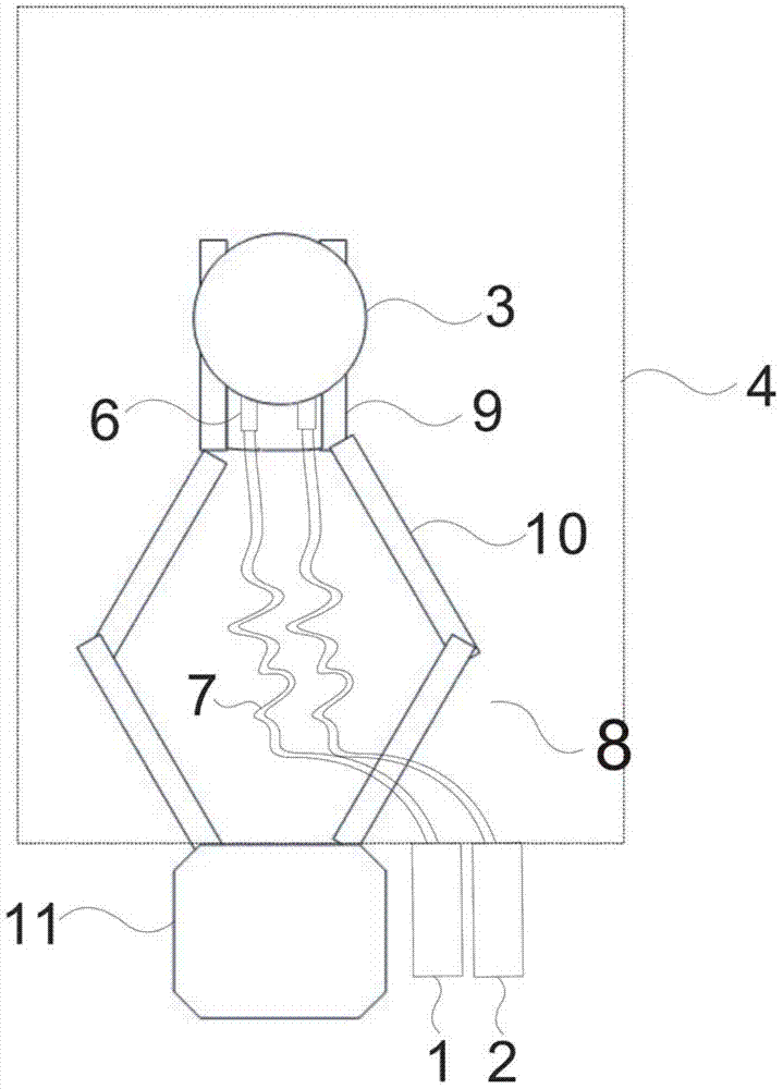
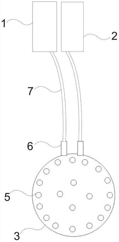
[0027] Combine below Figure 1 to Figure 4 The device for cleaning the wafer reaction chamber among the present invention is further described:

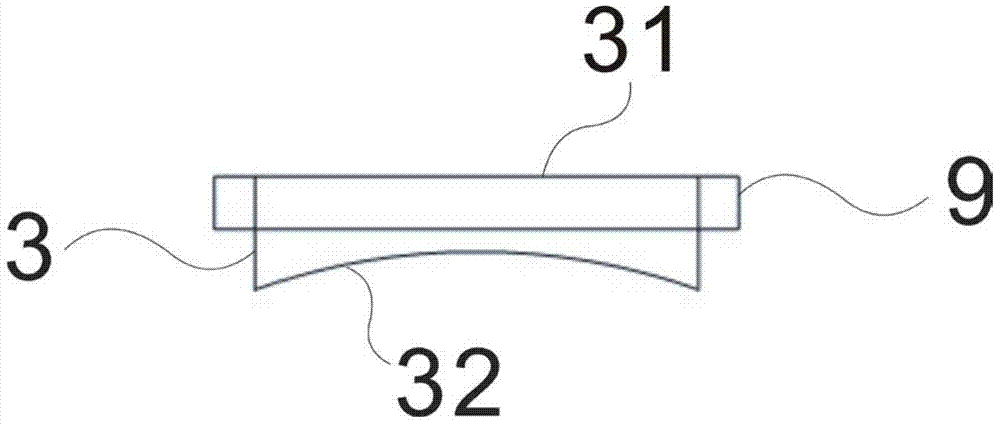
[0028] Such as figure 1 As shown, the present invention provides a device for cleaning a wafer reaction chamber, including a vacuum pump 1 and a nitrogen tank 2 outside the reaction chamber 4, including: a cleaning panel 3 installed in the reaction chamber 4 for cleaning Reaction chamber 4, several holes 5 are provided on the lower panel 32 of the cleaning panel 3, at least two interfaces 6 are provided at...


PUM


Abstract

The invention discloses a wafer reaction chamber cleaning device. The wafer reaction chamber cleaning device comprises arranging a vacuum pump and a nitrogen tank outside a reaction chamber and is composed of a cleaning facial disc and a mechanical hand, wherein the cleaning facial disc is arranged inside the reaction chamber and used for cleaning the reaction chamber and the lower facial disc of the cleaning facial disc is provided with a plurality of holes; the mechanical hand comprises a clamping unit, mechanical arms and a frame, the clamping unit is arranged at the ends of the mechanical arms and used for clamping the cleaning facial disc, the mechanical arms are movably mounted on the frame, and the clamping unit and the upper facial disc of the cleaning facial disc are connected through fixing units. The wafer reaction chamber cleaning device is simple in structure and convenient to use, can clean the reaction chamber by transmitting the cleaning facial disc through the mechanism arms without damaging the vacuum environment of the reaction chamber and further remove dirt inside the reaction chamber without opening and resetting the reaction chamber, thereby improving the technical progress during production application, saving the resetting time and reducing the rejection rate of wafers and the economic loss.

Description

technical field [0001] The invention relates to the field of semiconductor equipment, in particular to a device for cleaning a wafer reaction chamber. Background technique [0002] In the semiconductor process, it is necessary to carry out the corresponding process on the wafer in a confined space. With the upgrading of the semiconductor integrated circuit manufacturing process, the requirements for the vacuum degree and purity involved in the processing environment are getting higher and higher. Therefore, when the wafer is in a closed chamber environment, if contamination occurs in the reaction chamber, the contamination particles will pollute the chamber and cause the process to fail to proceed normally. [0003] The current solution is to open the cavity of the reaction chamber, re-clean the inside of the chamber, close the cavity after cleaning, make the cavity in a sealed state, and then perform vacuum operation. Since opening the chamber for cleaning has destroyed th...

Claims


Application Information

Patent Timeline
Patent Type & Authority Applications(China)
IPC IPC(8): H01L21/02
CPCB08B9/08B08B9/093
Inventor 顾晓冬
Owner SHANGHAI INTEGRATED CIRCUIT RES & DEV CENT
Why Eureka
Try Eureka