Fin field effect transistor and method of forming the same
A fin-type field effect and transistor technology, which is applied in semiconductor devices, semiconductor/solid-state device manufacturing, electrical components, etc., can solve problems such as inapplicability, achieve the effect of increasing driving current, increasing carrier mobility rate, and simple process
- Summary
- Abstract
- Description
- Claims
- Application Information
AI Technical Summary
Problems solved by technology
Method used
Image

Examples
Embodiment Construction
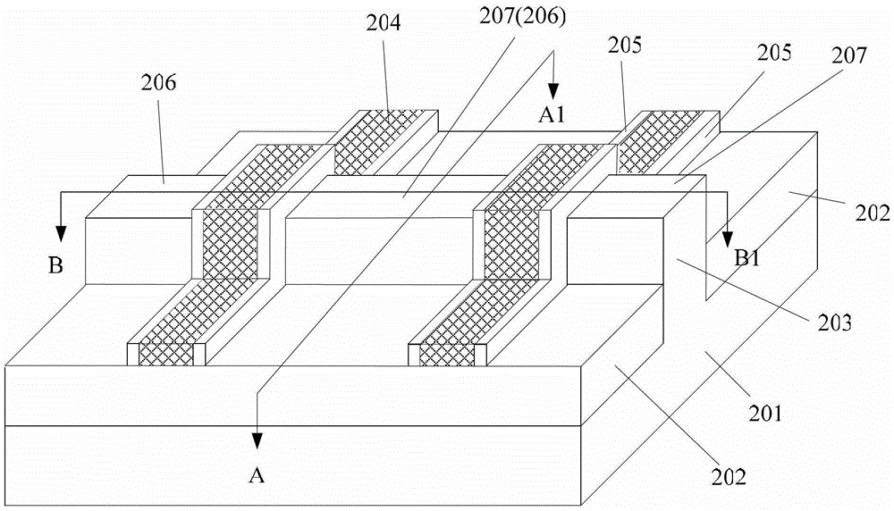
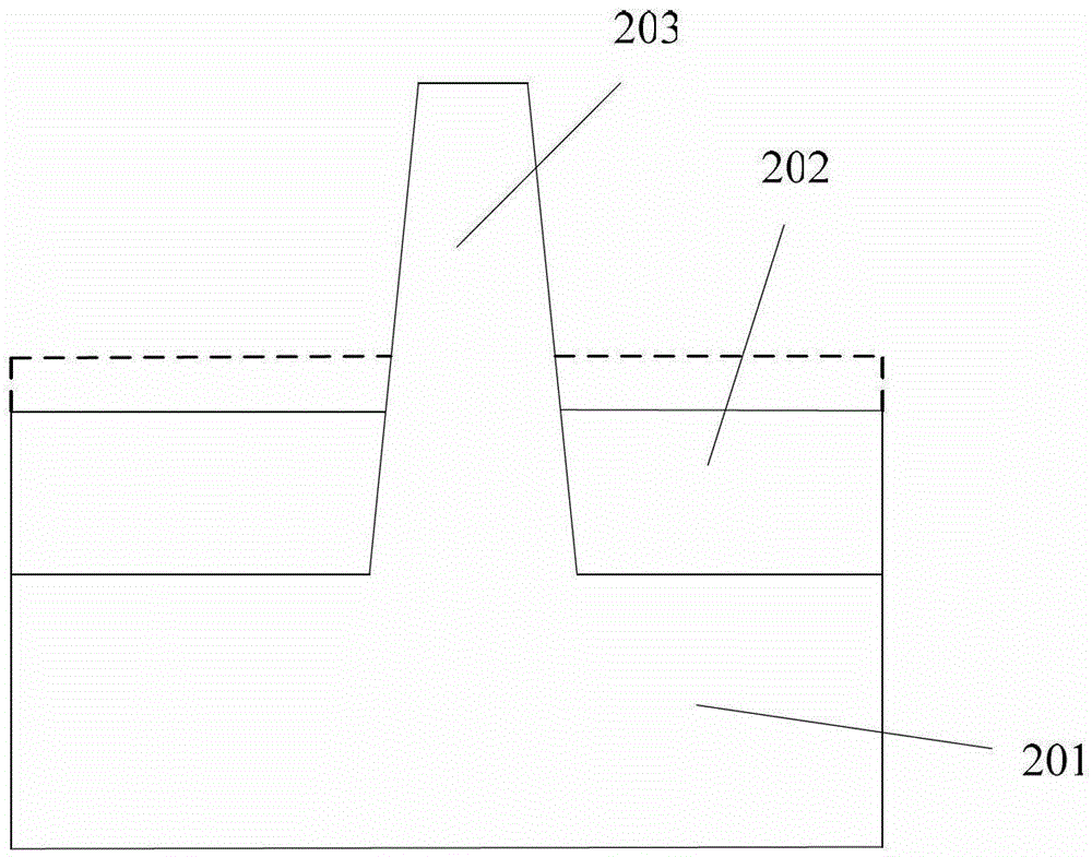
[0029] It can be known from the background art that in order to improve the performance of the fin field effect transistor device, stress can be introduced into the channel region of the MOS transistor to increase the mobility of carriers. However, with the development of semiconductor technology, such as the nitride capping layer (Nitride-Cap) stress layer, due to the high dielectric constant will increase the parasitic capacitance in the device, and the high parasitic capacitance will cause signal delay in the device and affect the chip performance. , so the use of the nitride cap layer stress layer is no longer suitable for highly integrated fin field effect transistor processes. The device performance of the fin field effect transistor in the prior art needs to be further improved.
[0030] In order to solve the above problems, the inventors of the present invention propose a method for forming a FinFET. The advantages of the present invention will become clearer by descr...
PUM
 Abstract
Description
Claims
Application Information
 - R&D
- Intellectual Property
- Life Sciences
- Materials
- Tech Scout
- Unparalleled Data Quality
- Higher Quality Content
- 60% Fewer Hallucinations
Browse by: Latest US Patents, China's latest patents, Technical Efficacy Thesaurus, Application Domain, Technology Topic, Popular Technical Reports.
© 2025 PatSnap. All rights reserved.Legal|Privacy policy|Modern Slavery Act Transparency Statement|Sitemap|About US| Contact US: help@patsnap.com