Frequency error detection device, frequency error detection method and receiving device
A frequency error and receiving device technology, which is applied in the field of frequency error detection devices, frequency error detection and receiving devices, can solve the problems of symbol timing error detection range limitation, lack of practicability, and large amount of IDFT calculations, etc., and achieve low power consumption , the effect of reducing the amount of computation
- Summary
- Abstract
- Description
- Claims
- Application Information
AI Technical Summary
Problems solved by technology
Method used
Image


Examples
Embodiment approach 1
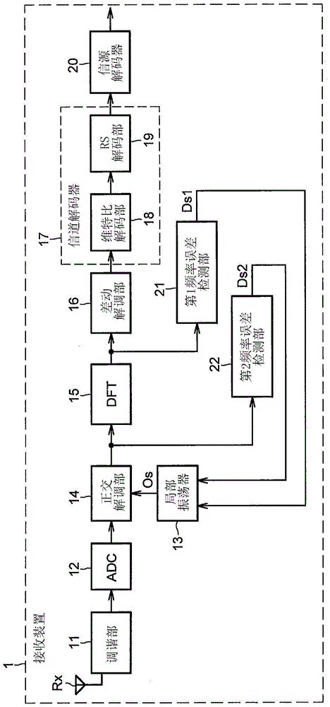
[0038] figure 1 It is a functional block diagram showing a schematic configuration of the receiving device according to Embodiment 1 of the present invention. Such as figure 1 As shown, the reception device 1 of the present embodiment includes a reception antenna element Rx, a tuner unit 11 , an A / D converter (ADC) 12 , a local oscillator 13 , and a quadrature demodulation unit 14 .
[0039] The tuner unit 11 receives radio signals via the receiving antenna element Rx. The tuner unit 11 performs analog signal processing such as tuning processing on the wireless signal to generate an analog reception signal of a carrier frequency band, and outputs the analog reception signal to the A / D converter 12 . The A / D converter 12 converts the analog reception signal in the carrier frequency band into a digital reception signal, and outputs it to the quadrature demodulation unit 14 . The digital reception signal is a multicarrier signal generated by digitally modulating and multiple...
Embodiment approach 2
[0104] Next, Embodiment 2 of the present invention will be described. Embodiment 2 is a modified example of Embodiment 1 described above. In Embodiment 1, the synchronization symbols corresponding to all N subcarriers are processed, but only synchronization symbols in a predetermined range of subcarriers can be processed. In this case, a further effect of reducing the amount of computation can be achieved. For example, when synchronous symbols corresponding to half of the N subcarriers are processed, the amount of computation can be further reduced to half.
[0105] Figure 10 is the sync symbol G(f that will correspond to every other subcarrier 0 ), G (f 2 ), G (f 4 ), G (f 6 ), ... as a graph of the state of the processing object. In this case, Figure 5 The first signal delay unit 46 delays the synchronization symbol serially input to the first complex arithmetic unit 32 by two subcarriers. When the synchronization symbol G (f k ), the first signal delay unit 46 o...
Embodiment approach 3
[0118] Next, Embodiment 3 of the present invention will be described. Figure 11 It is a functional block diagram showing a schematic configuration of the first frequency error detection unit 21B in the third embodiment. Such as Figure 11 As shown, the first frequency error detection unit 21B has a synchronization symbol extraction unit 31 , a first complex number calculation unit 32 , a reference signal supply unit 33B, a correlation calculation unit 36 and a peak detection unit 37 . The configuration of the reception device according to this embodiment is the same as that of the reception device 1 according to the first embodiment except for the first frequency error detection unit 21B.
[0119] Such as Figure 11 As shown, the reference signal supply unit 33B includes the above-mentioned reference complex signal R (f k ) of the signal storage unit 34B. The signal storage unit 34B can combine the multiplication signal D (f k ) corresponding to the reference complex s...
PUM
 Abstract
Description
Claims
Application Information