Method for producing a group iii nitride semiconductor

一种氮化物半导体、氮气氛的技术,应用在半导体/固态器件制造、气态化学镀覆、涂层等方向,达到降低制造成本的效果

Active Publication Date: 2014-04-02
TOYODA GOSEI CO LTD
View PDF5 Cites 13 Cited by
  • Summary
  • Abstract
  • Description
  • Claims
  • Application Information

AI Technical Summary

Problems solved by technology

[0005] However, the method disclosed in Japanese Laid-Open Patent Publication (Japanese Laid-Open) No. 2010-10363 requires a heat treatment process at a high temperature, and there is a problem of manufacturing cost

Method used


Image

  • Method for producing a group iii nitride semiconductor
  • Method for producing a group iii nitride semiconductor
  • Method for producing a group iii nitride semiconductor

Examples


Embodiment approach 1

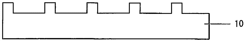
[0030] First, a sapphire substrate 10 having a c-plane main surface is prepared. One surface of the sapphire substrate was patterned by ICP dry etching ( Figure 1A ). The pattern includes a dot pattern or a stripe pattern in which depressions and projections are periodically arranged. In the case of dot patterns, each dot has hexagonal, rectangular, triangular, circular and other planar shapes and cones, cones, prisms, cylinders, truncated pyramids having the above-mentioned planar shapes on the top surface of the dots, respectively , truncated cones, and other three-dimensional shapes.

[0031] The depth of the pattern (the height of the protrusions of the dot pattern, the depth of the depressions of the dot pattern, or the depth of the stripe grooves) is preferably 0.1 μm to 10 μm. When the depth is less than 0.1 μm, the light extraction efficiency is not sufficiently improved in the light emitting device according to the present invention. When the depth exceeds 10 μm,...

Embodiment approach 2

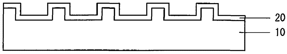
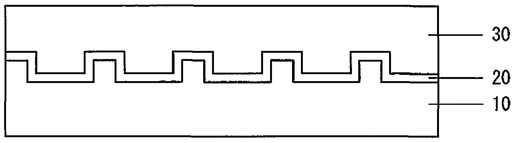
[0040] The manufacturing method of the Group III nitride semiconductor according to Embodiment 2 is the same as the manufacturing method according to Embodiment 1 except that the heat treatment is not performed before the buffer layer 20 is formed. That is, after the sapphire substrate 10 is patterned, the temperature is maintained at normal temperature without heat treatment, and the AlN buffer layer 20 is formed by magnetron sputtering.

[0041] The method for manufacturing Group III nitride semiconductor layer 30 according to Embodiment 2 also allows formation of Group III nitride semiconductor having good surface flatness and crystallinity, similarly to the case according to the manufacturing method in Embodiment 1. In addition, since heat treatment is not performed, the manufacturing process can be simplified and the manufacturing cost can be reduced. This is because the sapphire substrate 10 is heated by magnetron sputtering instead of the heat treatment before the buffe...

Embodiment approach 3

[0044] Such as Figure 6A As shown, a sapphire substrate 11 having a c-plane main surface was prepared. One surface of the sapphire substrate was patterned into periodic concave and convex patterns by ICP dry etching. The shape, size and recess depth of the pattern are the same as those according to Embodiment 1.

[0045] Subsequently, patterned sapphire substrate 11 is subjected to heat treatment at a temperature higher than 800° C. to 1100° C. in a nitrogen or hydrogen atmosphere. The pressure is normal pressure. During the heat treatment, immediately after heating to the designed temperature, the heating is stopped to lower the temperature to normal temperature. Heat treatment may be performed using magnetron sputtering or other devices used in subsequent processes.

[0046] Next, the patterned sapphire substrate 11 was placed in the chamber of a magnetron sputtering device. As the sapphire substrate 11 is heated from 200° C. to below 700° C., an AlN buffer layer 21 is...


PUM


Abstract

The surface of a sapphire substrate having a c-plane main surface is patterned by ICP dry etching. The patterned sapphire substrate is thermally treated in a hydrogen or nitrogen atmosphere at a temperature of less than 700 DEG C. or at a temperature of more than 800 DEG C. to 1100 DEG C. An AlN buffer layer is formed by magnetron sputtering on the surface on the patterned side of the sapphire substrate heated at a temperature of 200 DEG C. to less than 700 DEG C. On the buffer layer, a Group III nitride semiconductor layer having a c-plane main surface is formed so as to have a thickness of 1 [mu]m to 10 [mu]m by MOCVD.

Description

technical field [0001] The present invention relates to a method of forming a Group III nitride semiconductor by MOCVD after forming an AlN buffer layer on a patterned sapphire substrate by sputtering. Background technique [0002] Since the lattice constant of sapphire is significantly different from that of the Group III nitride semiconductor when the Group III nitride semiconductor is formed on the sapphire substrate using MOCVD, a buffer layer is formed between the sapphire substrate and the Group III nitride semiconductor to reduce Lattice mismatch, thereby improving the crystallinity of the Group III nitride semiconductor. Generally, the buffer layer is made of AlN or GaN grown at low temperature by MOCVD, but a technique of forming the buffer layer by sputtering is also known. [0003] In the method for manufacturing a Group III nitride semiconductor light emitting device, a Group III nitride semiconductor layer is formed on a patterned sapphire substrate via a buffe...

Claims


Application Information

Patent Timeline
Patent Type & Authority Applications(China)
IPC IPC(8): H01L21/205
CPCC23C16/0218C23C16/0272H01L21/0242H01L21/02576C23C16/303H01L21/0254H01L21/02658H01L21/02365H01L21/0262H01L21/0243H01L21/02631H01L21/02579H01L21/02458
Inventor 中田尚幸
Owner TOYODA GOSEI CO LTD
Why Eureka
Try Eureka